Organic electroluminescence display device

Active Publication Date: 2006-06-20
SAMSUNG DISPLAY CO LTD +1
View PDF9 Cites 47 Cited by
  • Summary
  • Abstract
  • Description
  • Claims
  • Application Information

AI Technical Summary

Benefits of technology

[0012]In the present invention, the filler can comprise a desiccant dispersed with fine metallic particles to have increased thermoconductivity and electroconductivity. This can simultaneously solve the problems of preventing moisture inflow into the p

Problems solved by technology

However, they do not sufficiently recognize improvement of thermoconductivity of a display device to efficiently radiate heat generated therein or improvement of electroconductivity of an electroconductive layer which constitutes an OLED a

Method used


Image

  • Organic electroluminescence display device
  • Organic electroluminescence display device
  • Organic electroluminescence display device

Examples


Example

EXAMPLE 1

[0064]The material having the following composition is used as one example of the filler for the embodiment of the present invention:

Filler 1

[0065]ComponentsCompositionEpoxy resin100 parts by weight Amine type curing agent30 parts by weightCu particles40 parts by weightCaO particles 5 parts by weightCoupling agent0.1 parts by weight 

[0066]The epoxy resin may be a bisphenol A type resin commercially available, which is liquid at room temperature. A bisphenol A type epoxy resin is suitable because it makes the filler spreadable on a surface, and also preferable for preparation of a printing ink, as described later. The amine curing agent may be selected from various aliphatic or aromatic amine adducts. Curing agents of anhydrous acids or thiol-based one can be used by the related industries. The Cu particles are incorporated to impart thermoconductivity and electroconductivity to the filler. The fine metallic Cu particles having a size of around 1 μm can be used. The CaO part...

Example

EXAMPLE 2

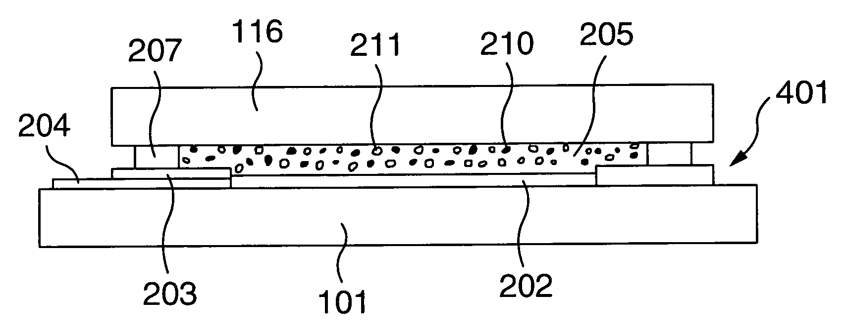
[0072]A method adopted in this embodiment for applying the filler to encapsulating the OLED is described by referring to FIGS. 4 and 5. The filler 205 having the composition shown in EXAMPLE 1 is spread by screening printing on the pixel area 202 and insulator 203 on the OLED substrate 401 on which the transistor active matrix is formed by polysilicon on the glass substrate 101. The filler can be spread to a thickness which is controlled at 20 to 50 μm by use of a 300-mesh screen printing plate. The glass substrate for the encapsulating plate 116 is put on the filler, on completion of the printing work, to prevent bubbles from being drug onto the filler, and the filler is cured under heating at 120° C. for 30 minutes. All of the printing, placing the glass substrate and curing works are preferably carried out in a glove box completely free of mixture. It is recommended that moisture is removed to decrease dew point of −60° C. or lower in the glove box.

[0073]This embodiment ...

Example

EXAMPLE 3

[0074]Another method adopted in this embodiment for applying the filler to encapsulating the OLED is described by referring to FIG. 6. The filler 205 having the composition shown in EXAMPLE 1 is spread by screening printing on the pixel area 202 and insulator 203 on the OLED substrate 401 on which the transistor active matrix is formed by polysilicon on the glass substrate 101. The filler can be spread to a thickness which is controlled at 20 to 50 μm by use of a 300-mesh screen printing plate. On completion of the printing work, the seal 207 is spread by a dispenser or the like to a width of 2 mm on the insulator 203 in such a way to cover the periphery of the filler 205. An UV curing type may be used for the seal 207. Then, the glass substrate for the encapsulating plate 116 is put on the filler 205 and seal 207, on completion of the printing work, to prevent bubbles from being drug onto them, the seal 207 portion is selectively irradiated with UV to be cured, and the fil...


PUM

PropertyMeasurementUnit
Percent by massaaaaaaaaaa
Lengthaaaaaaaaaa
Particle sizeaaaaaaaaaa

Abstract

An OLED display device having a laminate encapsulating structure containing: an OLED substrate having a leading wire and a pixel area which carries a number of OLEDs on a glass substrate; and an encapsulating plate; and a filler filling a space between the OLED substrate and the encapsulating plate, wherein the filler is dispersed with a desiccant and fine metallic partides for improving electroconductivity and thermoconductivity. This structure not only can prevent an inflow of moisture into the OLEDs and secure a mechanical strength of the OLED display device as a flat panel display device, but also accelerate a heat radiation and improves electroconductivity of a conductive layer.

Description

FIELD OF THE INVENTION[0001]The present invention relates to a flat panel display device, in particular an organic electro-luminescence display device, a pixel of which is composed of an organic light emitting diode (OLED).BACKGROUND OF THE INVENTION[0002]Attempts have been made in the technical development for commercializing flat panel display devices which use OLEDs to prevent moisture-caused deterioration of OLED characteristics, and to partly solve problems involved in means for securing mechanical strength associated with flat panel display devices. For example, JP-A-9-148066 discloses use of a desiccant; JP-A-8-236271 discloses a structure with a gap between a substrate which constitutes an OLED and encapsulating can (or plate) filled with a rubber elastomer to prevent inflow of moisture; JP-A-5-182759 discloses a structure with a gap between a substrate which constitutes an OLED and encapsulating plate filled with an UV curing resin; and JP-A-2001-68266 discloses a structure...

Claims


Application Information

Patent Timeline
IPC IPC(8): H05B33/04H01L51/50H01L27/32H01L51/52H05B33/14
CPCH01L51/5237H01L51/529H01L27/3244Y10T428/25H01L2251/5315Y10S428/917H10K59/12H10K50/846H10K50/8426H10K50/87H10K2102/3026
Inventor KIKUCHI, HIROSHIUSHIFUSA, NOBUYUKITAKEMOTO, ISSEI
Owner SAMSUNG DISPLAY CO LTD
Why Eureka
Try Eureka