Display device and electronic apparatus

a technology of electronic equipment and display device, which is applied in the direction of semiconductor devices, instruments, optics, etc., can solve the problems of further thus narrowing the effective display region of the device, so as to achieve stable supply of drive control signals, effective utilization of the surface area of the substrate, and effective utilization of the non-display region

Active Publication Date: 2006-06-27
ELEMENT CAPITAL COMMERCIAL CO PTE LTD
View PDF21 Cites 11 Cited by
  • Summary
  • Abstract
  • Description
  • Claims
  • Application Information

AI Technical Summary

Benefits of technology

[0015]Also preferably, in the display device of the invention, the surface of the insulating layer may be formed of a material having an affinity for the essential display layer that is relatively higher than an affinity of the surface of each barrier. This embodiment is almost free from a problem that the thickness of the essential display layer may increase around the barriers, or the essential display layer may be more uniform in this embodiment. As a result, this embodiment will be almost free from a trouble of contrast reduction.
[0016]Also preferably in the display device of the invention, the substrate may be provided thereon with multiple scanning lines and multiple data lines formed to cross each other, the switch unit is connected to the scanning lines and the data lines, and the operation control unit includes a data control unit to control the signal to run through the data lines. Apart from this, the switch unit may be connected to the scanning lines and the data lines, and the operation control unit may include a scanning control unit to control the signal to run through the scanning lines. Needless-to-say, the operation control unit may include both the data control unit and the scanning control unit. Also preferably, the substrate may be provided thereon with multiple inspection lines, the switch unit is connected to the inspection lines, and the operation control unit includes an inspection control unit to control the signal to run through the inspection lines. Needless-to-say, the operation control unit may include the data control unit,

Problems solved by technology

In such display devices, the driving circuits and/or control circuits must be mounted on their substrate, and this causes various problems in that the substrate is large sized, and not much of the region having these circuits can be used for the display region of the devices, and the effective display region of the devices is thereby narrowed.
In

Method used


Image

  • Display device and electronic apparatus
  • Display device and electronic apparatus
  • Display device and electronic apparatus

Examples


Embodiment Construction

[0028]Exemplary embodiments of the invention are described hereinunder with reference to the drawings attached hereto. The exemplary embodiments demonstrate some preferred embodiments of the invention and do not whatsoever restrict the invention. The exemplary embodiments may be modified in any desired manner within the technical scope of the invention. In the drawings referred to hereinunder, the layers and the members that constitute the illustrated devices are scaled down differently from their actual scale in order to be well recognizable in the drawings.

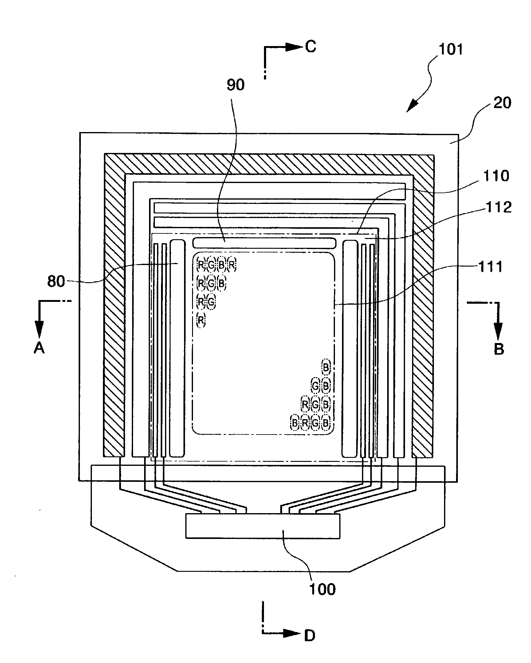
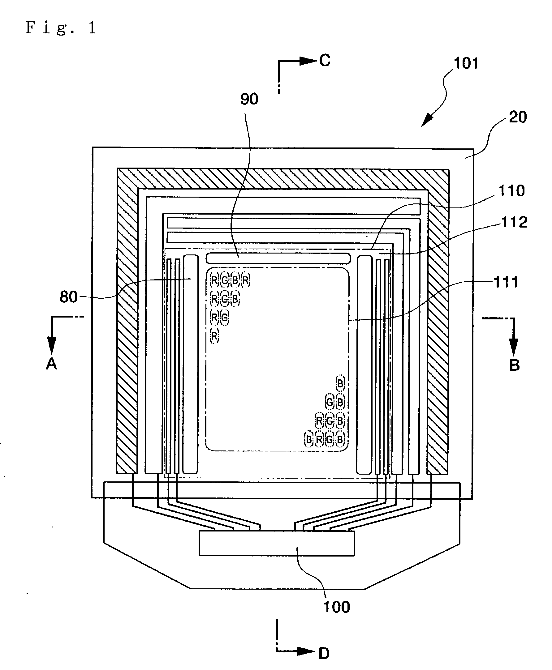
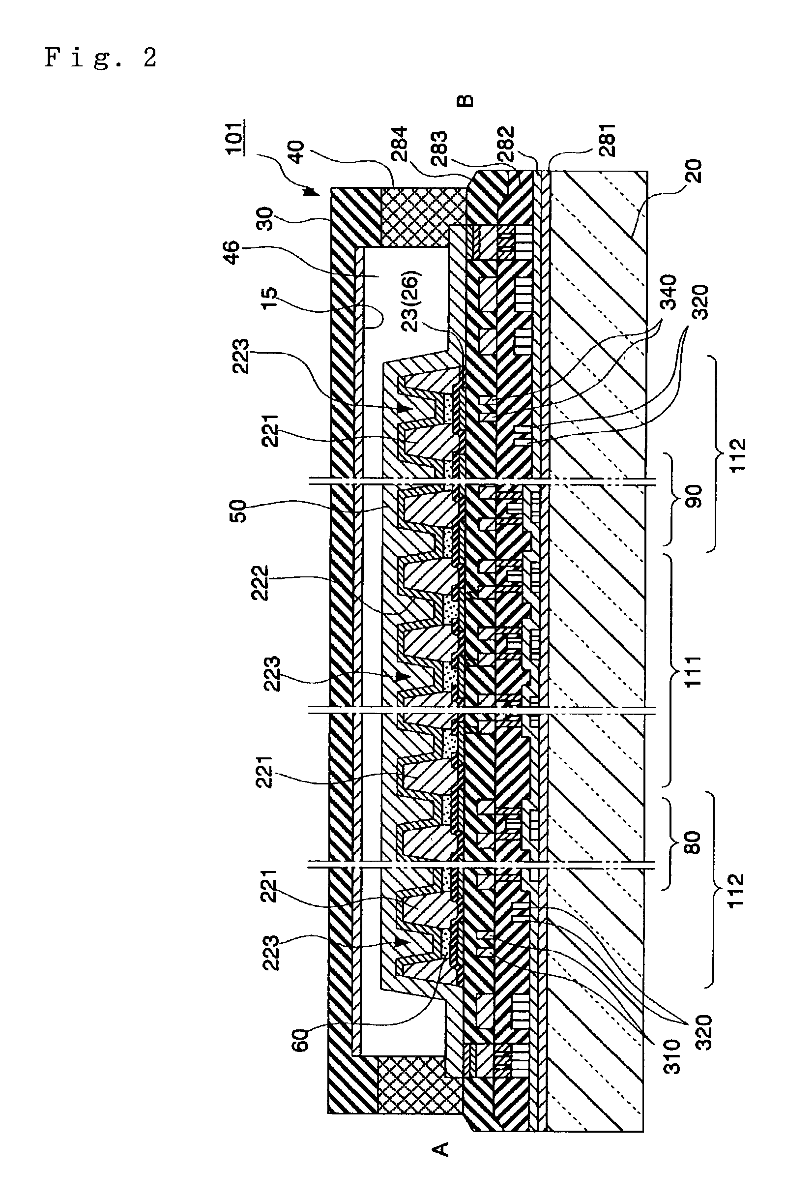
[0029]An embodiment of the invention that is applied to an EL display in which the electro-optical substance to form the essential display layer is an electroluminescent (EL) substance is described first. FIG. 1 and FIG. 2 are a plan view and a cross-sectional view taken along plane A-B, respectively, and schematically show the constitution of the EL display device of this embodiment. The EL display device 101 shown in FIGS. 1 a...


PUM


Abstract

The invention provides a display device and an electronic apparatus that incorporates the display device. The display device has drive control signal lines to control driving circuits and others thereof in a predetermined site of the substrate to thereby increase the effective display region of the surface of the substrate. The display device is free from, or is protected from, external influences on the drive control signals that pass through it. A predetermined matrix pattern of a bank layer and a recess region of which the recesses are spaced from each other with the banks adjacent thereto of the bank layer, are formed on a substrate. A real pixel region for display and a dummy pixel region not for display are formed in the pixel region to be a display region of the substrate. A scanning line-driving circuit to control the output of scanning signals that pass through scanning lines, and a drive control signal conduction element through which drive control signals pass to drive the scanning line-driving circuit, are also formed on the substrate. In the plan view of the substrate, the drive control signal conduction element is superimposed at least partly on the bank layer of the dummy pixel region.

Description

BACKGROUND OF THE INVENTION[0001]1. Field of Invention[0002]The invention relates to a display device and an electronic apparatus.[0003]2. Description of Related Art[0004]Some related art optical display devices, such as liquid-crystal display devices and EL display devices, have a layered structure of multiple circuit elements, electrodes and liquid-crystal or EL elements layered on a substrate. For example, a type of such an EL display device has a sandwich structure of a light-emitting substance containing, light-emitting layer sandwiched between electrode layers of an anode and a cathode, in which the holes from the anode are recombined with the electrons from the cathode in the light-emitting layer having the ability of fluorescence emission. The device of the type emits light while it is not activated from its excited condition, and this is the phenomenon of the device to emit light.[0005]A related art active matrix driving system can be used to drive the EL display device tha...

Claims


Application Information

Patent Timeline
IPC IPC(8): G09G3/30G02F1/1362H01L27/32
CPCG02F1/13454H01L27/3276H01L27/3246H01L27/3223H10K59/88H10K59/122H10K59/131G09G3/30
Inventor NAKANISHI, HAYATO
Owner ELEMENT CAPITAL COMMERCIAL CO PTE LTD
Why Eureka
Try Eureka