Supercharge Your Innovation With Domain-Expert AI Agents!

Universal test fixture

a test fixture and universal technology, applied in the direction of electronic circuit testing, measurement devices, instruments, etc., can solve the problems of reducing the throughput of the tester, the design and fabrication of the test fixture has become more complicated, and the target on the pcb is difficult to meet the requirements, so as to achieve the effect of high speed

Inactive Publication Date: 2006-07-04
AGILENT TECH INC
View PDF16 Cites 7 Cited by
  • Summary
  • Abstract
  • Description
  • Claims
  • Application Information

AI Technical Summary

Benefits of technology

The invention provides a universal fixture that can quickly test electronic devices like printed circuit boards. It has multiple contact points that can be selected based on the position of the target on the device. This allows for quick and efficient testing of electronic devices.

Problems solved by technology

In addition, with decreasing component size, the design and fabrication of the test fixtures has become more complicated.
As a result, the cost of producing the test fixtures has significantly increased.
Although the “flying probe” tester permits testing of high resolution PCBs, the serial approach of testing targets on a PCB reduces the throughput of the tester.

Method used


Image

  • Universal test fixture
  • Universal test fixture
  • Universal test fixture

Examples


Embodiment Construction

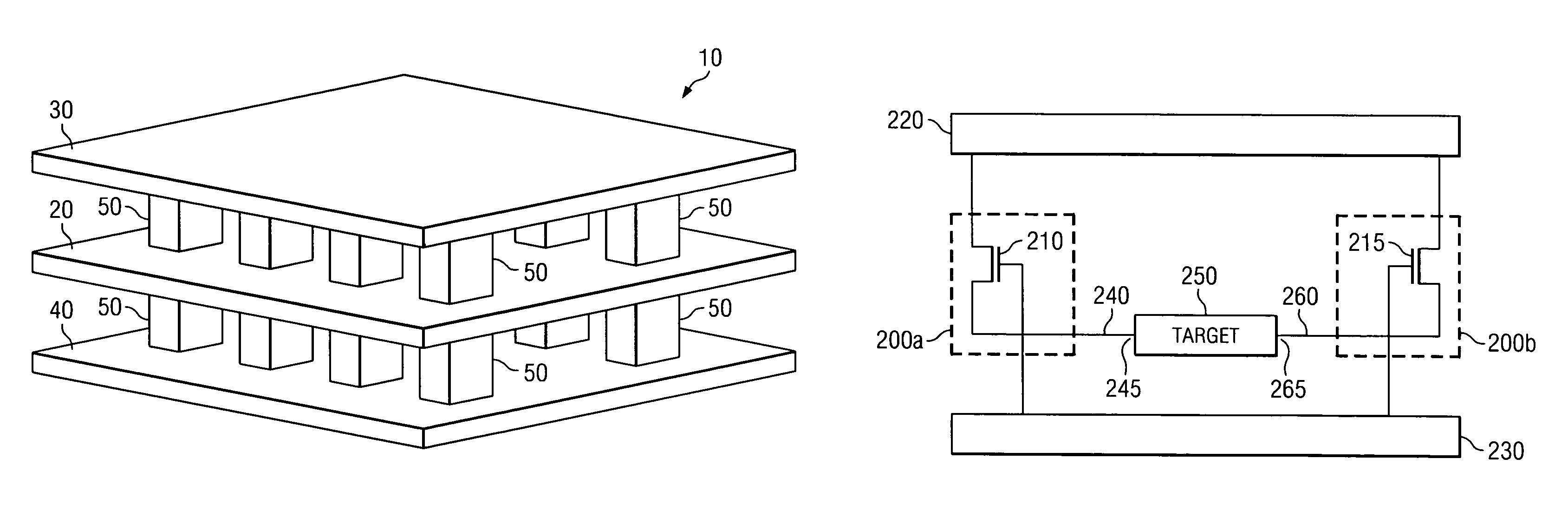
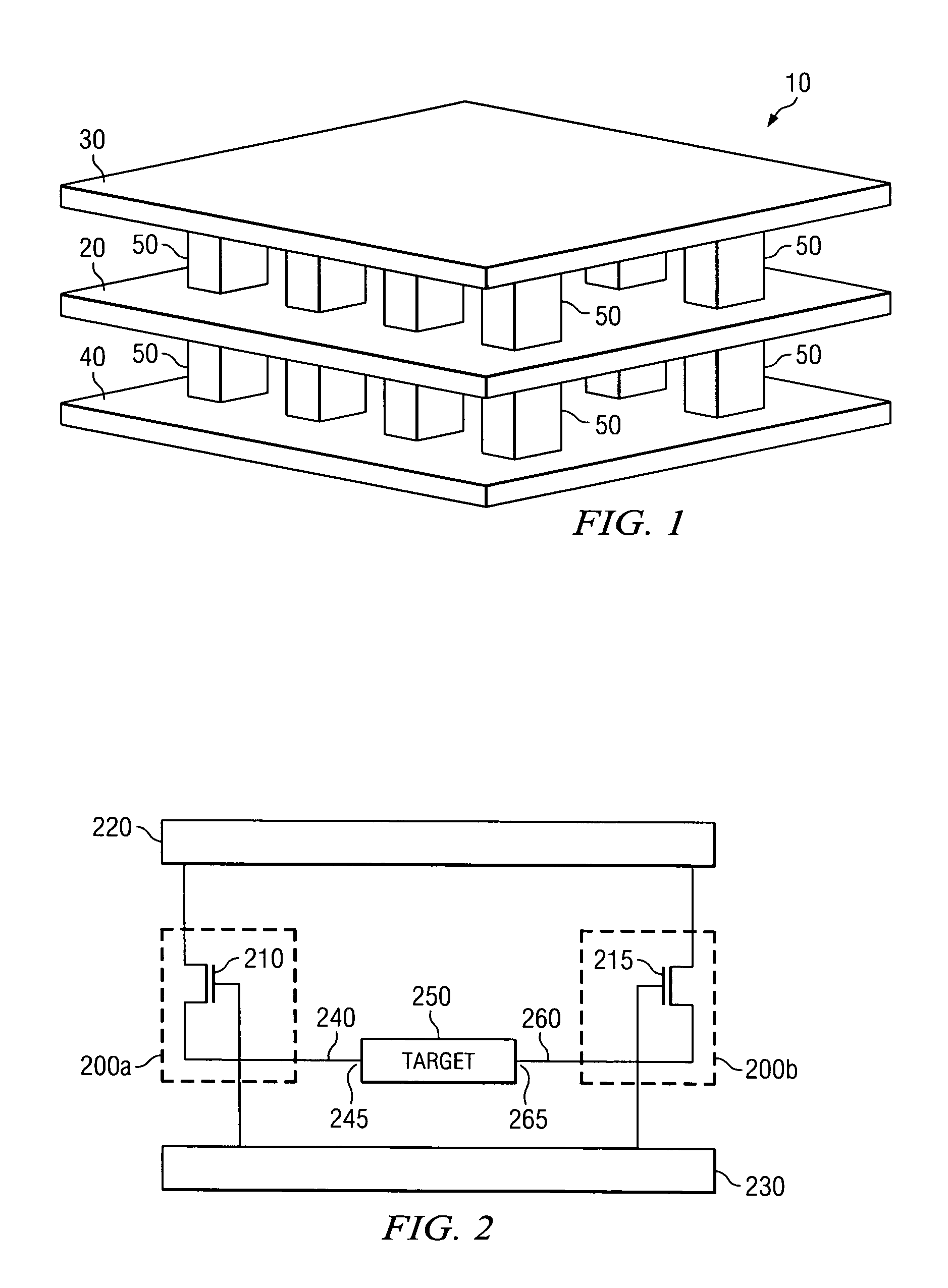
[0017]Embodiments in accordance with the invention provide a universal fixture, testing system and a method for testing electronic devices, such as bare printed circuit boards (PCBs). The universal fixture is capable of testing PCBs at rates of speed greater than those achievable by traditional “flying probe” testers.

[0018]FIG. 1 is a top perspective view of a testing assembly including universal fixtures for testing an electronic device according to an exemplary embodiment in accordance with the invention. The testing assembly is generally designated by reference number 10 and includes first universal fixture 30 and second universal fixture 40. An electronic device 20, such as a bare PCB, is sandwiched between first universal fixture 30 and second universal fixture 40. First universal fixture 30 is placed in direct contact with one side of PCB 20, while second universal fixture 40 is placed in direct contact with the other side of PCB 20.

[0019]Each universal fixture 30 and 40 inclu...


PUM


Abstract

A universal fixture for testing a device, such as a bare printed circuit board, includes a plurality of addressable contact points. Each of the contact points includes a switch connected to a conductor capable of creating an electrical connection to the device. To obtain a measurement of a target on the device, two of the contact points on the universal fixture are selected based on the position of the target on the device relative to the contact points.

Description

DESCRIPTION OF RELATED ART[0001]Before a printed circuit board (PCB) is loaded with components, the testpads, vias, traces and plated through-holes on the bare PCB are tested for electrical connectivity and continuity. Typical measurements conducted by bare-board testers include shorts, opens and impedance or resistance. Most conventional bare-board testers fall into one of two categories, either a “bed of nails” tester or a “flying probe” tester.[0002]A “bed of nails” tester is used on low resolution PCBs that have line and space widths of 250 μm or greater. The “bed of nails” tester utilizes a bare-board fixture containing a series of plastic sheets with holes drilled to permit passage of pins (nails). During testing, the PCB is placed in direct contact with the bare-board fixture. The pins on the fixture connect the various targets (e.g., testpads, vias, traces and through-holes) on the PCB to the internal electronics of the tester. Although, the “bed of nails” tester permits nea...

Claims


Application Information

Patent Timeline
Patent Type & Authority Patents(United States)
IPC IPC(8): G01R31/02
CPCG01R1/07385G01R1/07328G01R1/07335
Inventor HOKE, CHARLES D.NISHIMURA, KEN A.
Owner AGILENT TECH INC
Features
  • R&D
  • Intellectual Property
  • Life Sciences
  • Materials
  • Tech Scout
  • Unparalleled Data Quality
  • Higher Quality Content
  • 60% Fewer Hallucinations
Learn More