NOR flash memory device and method of shortening a program time

a technology of flash memory and program time, applied in the field of flash memory devices, can solve the problems of increasing the overall time to program the entire memory cell, and inevitable to have a limit in the number of bits programmable in a given time, and achieve the effect of shortening the tim

Inactive Publication Date: 2006-07-04
SAMSUNG ELECTRONICS CO LTD
View PDF7 Cites 23 Cited by
  • Summary
  • Abstract
  • Description
  • Claims
  • Application Information

AI Technical Summary

Benefits of technology

[0010]A plurality of program data composed of word units is programmed at the same time, so that the time for programming the whole memory cell array can be shortened.

Problems solved by technology

However, it is inevitable to have a limit in the number of bits programmable in a given time because such a charge pump circuit occupies a large circuit area.
Further, according to trends, increased memory capacity leads to an overall increase of time to program the entire memory cells.

Method used


Image

  • NOR flash memory device and method of shortening a program time
  • NOR flash memory device and method of shortening a program time
  • NOR flash memory device and method of shortening a program time

Examples


Embodiment Construction

[0029]Preferred embodiments of the present invention will be described below in more detail with reference to the accompanying drawings. The present invention may, however, be embodied in different forms and should not be constructed as limited to the embodiments set forth herein. Rather, these embodiments are provided so that this disclosure will be thorough and complete, and will fully convey the scope of the invention to those skilled in the art. Like numerals refer to like elements throughout the specification.

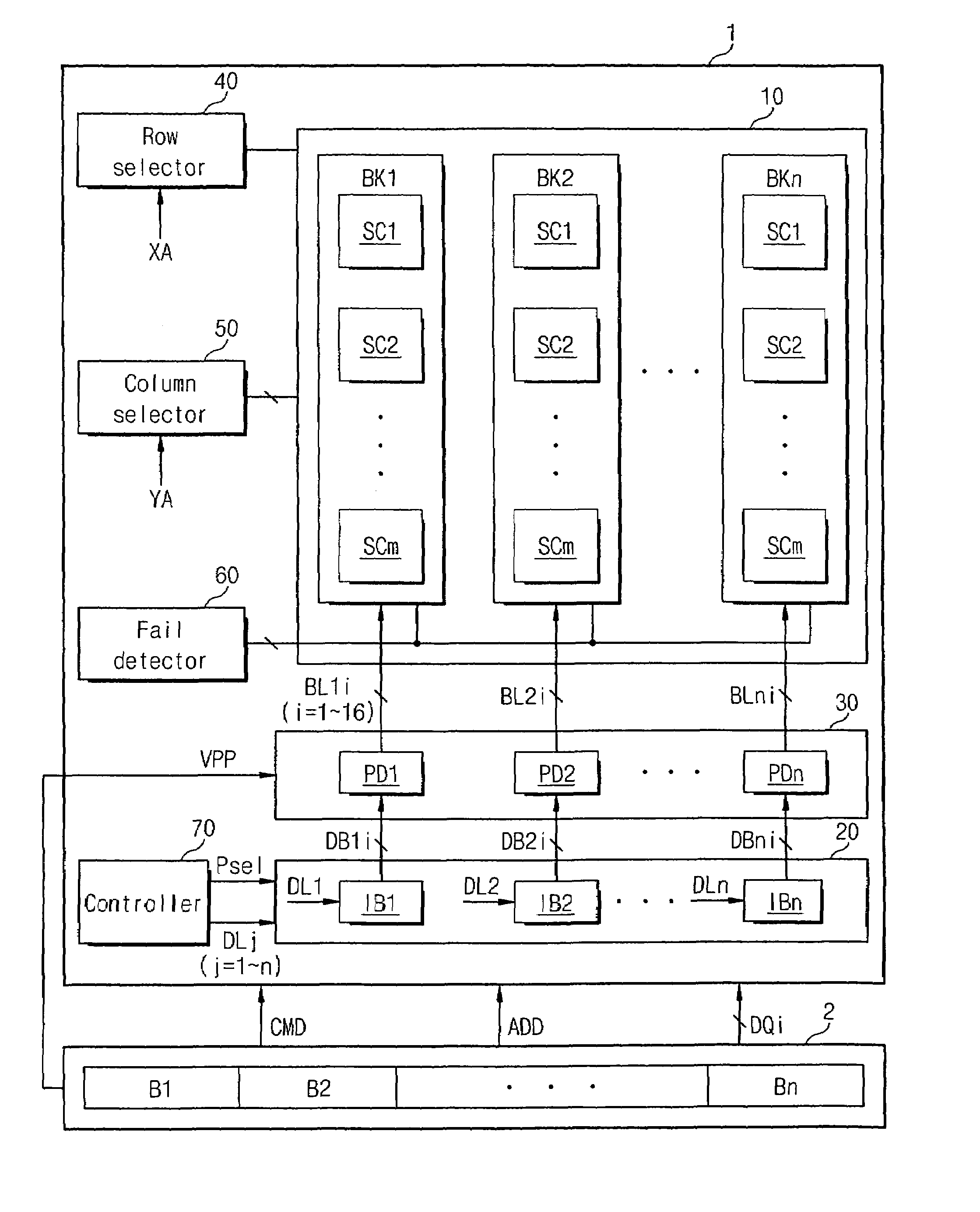
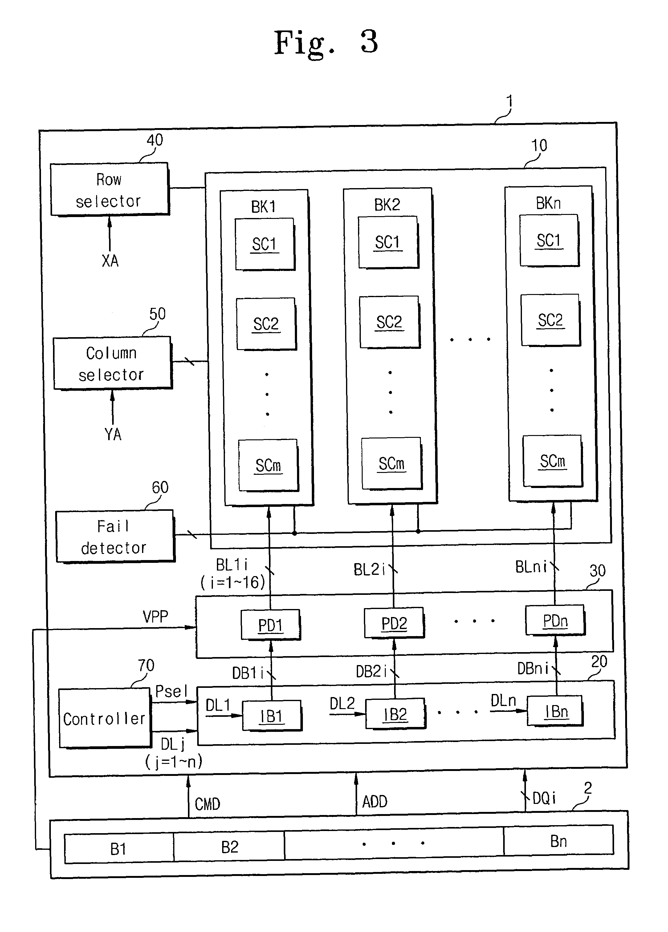
[0030]FIG. 3 is a block diagram illustrating an embodiment of a NOR flash memory device in accordance with the present invention. Referring to FIG. 3, the NOR flash memory device 1 according to the invention is comprised of a cell array 10, a row selector 40, and a column selector 50.

[0031]The cell array 10 is composed of a plurality of banks BK1˜BKn. Each bank is composed of a plurality of sectors SC1˜SCm each as a unit of erasing. Each sector is constructed of a pluralit...


PUM


Abstract

A NOR flash memory device is capable of shortening a program time. Included is a cell array segmented into a plurality of banks, a data input buffer to receive and store data composed of units of words, the number of units corresponding to the number of banks, and a program driver to apply a program voltage contemporaneously to the banks. According to the present invention, a plurality of program data composed of word units is programmed at the same time, so that the time for programming the whole memory cell array can be shortened.

Description

CROSS-REFERENCE TO RELATED APPLICATIONS[0001]This U.S. non-provisional patent application claims priority under 35 U.S.C. § 119 of Korean Patent Application 2004-24600 filed on Apr. 9, 2004, the entire contents of which are hereby incorporated by reference.BACKGROUND OF THE INVENTION[0002]The present invention is relevant to NOR flash memory devices, in particular to programming data into the NOR flash memory devices.[0003]Flash memory devices are usually classified into NAND and NOR types. The NAND flash memory device has a structure of strings, in which a plurality of memory cells is connected from a single bitline in series. On the other side, the NOR flash memory device is constructed of a plurality of memory cells connected to a single bitline in parallel.[0004]FIG. 1 shows a section of a memory cell employed in a flash memory device. As illustrated in FIG.1, a flash memory cell is composed of a source region 3 and a drain region 4 that are formed in a P-type substrate 9, a flo...

Claims


Application Information

Patent Timeline
Patent Type & Authority Patents(United States)
IPC IPC(8): G11C16/04G11C8/12G11C11/34G11C16/10G11C16/12
CPCG11C8/12G11C16/10G11C16/0416A01G9/023A01G9/024A01G9/028A01G9/042A01G9/124A01G27/005A47G7/041
Inventor JEONG, JAE-YONGLIM, HEUNG-SOO
Owner SAMSUNG ELECTRONICS CO LTD
Why Eureka
Try Eureka