Site control for OPC

a site control and opc technology, applied in the field of layout verification methods, can solve the problems of optical distortion, poor or unexpected output of opc tools,

Active Publication Date: 2006-07-04
SIEMENS PROD LIFECYCLE MANAGEMENT SOFTWARE INC
View PDF28 Cites 102 Cited by
  • Summary
  • Abstract
  • Description
  • Claims
  • Application Information

AI Technical Summary

Problems solved by technology

As the size of objects being created on a wafer approaches and becomes smaller than the wavelength of light used to expose the wafer, optical distortions can occur such that the pattern of objects defined by the mask or reticle will not match the pattern of objects that are created on the wafer.
In some cases, where certain features cannot or can barely be resolved with a particular lithographic process, the placement or presence of certain control sites in a polygon can cause the OPC tool to produce poor or unexpected results. FIG. 1B illustrates an example wherein an OPC tool attempts to adjust the position of the edge segments such that the edge placement error at each control site is minimized.

Method used


Image

  • Site control for OPC
  • Site control for OPC
  • Site control for OPC

Examples


Embodiment Construction

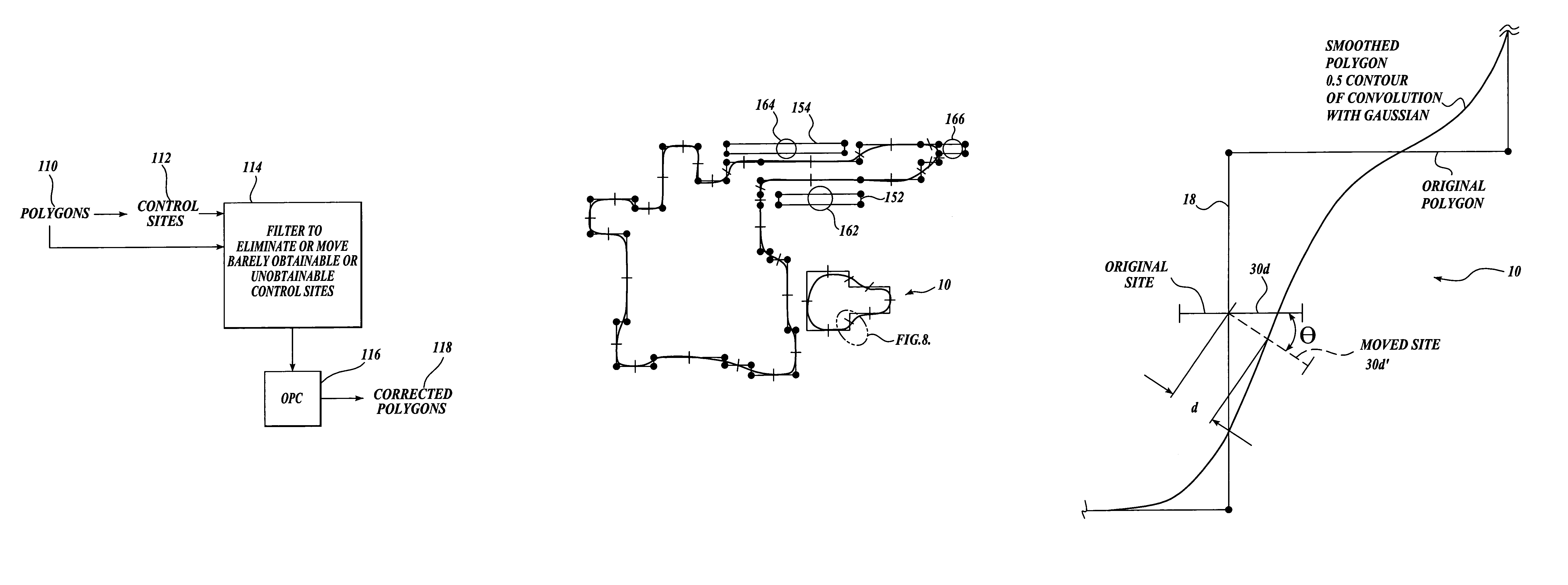
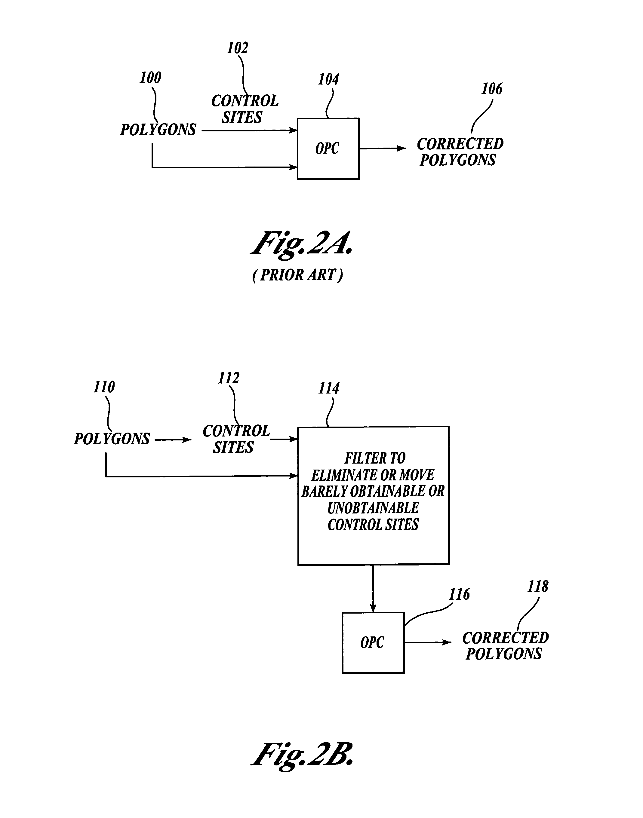
[0021]FIG. 2A illustrates a conventional method for applying an optical and process control (OPC) tool to a file that defines objects to be created on a semiconductor wafer. The objects to be created are typically defined in the file as polygons 100 in a layout language such as GDSII or OASIS. The polygons are fragmented by a computer into a number of edge segments that extend around the perimeter of each polygon. In addition, control sites 102 are defined where the edge placement error (EPE) for each edge segment should be minimized or zero, as well as where measurements of simulated process parameters in the area of the edge segment are to be made. Control sites are generally oriented in a direction that is normal to the length of the edge segment. The initial position of the control sites can be made by rules, such as placing the control site at the middle of each edge segment. Also, rules may determine that some edge segments may be too short to have a control site.

[0022]The fra...


PUM

PropertyMeasurementUnit
perimeteraaaaaaaaaa
distanceaaaaaaaaaa
angleaaaaaaaaaa

Abstract

A method for processing objects to be created via photolithography. Each object to be created is defined as a polygon that is fragmented into a number of edge segments that extend around the perimeter of the polygon. At least some of the edge segments have an associated control site where the edge placement error for the edge segment is to be minimal. A smoothing filter is applied to the polygon to identify those control sites that may cause an OPC tool to produce erroneous results. The identified control sites are moved and / or eliminated from the polygon, and polygon and the adjusted control sites are supplied to an OPC tool.

Description

FIELD OF THE INVENTION[0001]The present invention relates to layout verification methods in general, and in particular to methods for enhancing the fidelity of objects to be created with a photolithographic process.BACKGROUND OF THE INVENTION[0002]In conventional photolithographic processing, objects are created on a semiconductor wafer by exposing the wafer with light that is passed through a mask or reticle. The mask / reticle has patterns of opaque and clear areas that selectively expose light sensitive chemicals on the wafer. The chemicals are processed to selectively remove portions of a layer, thereby creating the desired structures on the wafer.[0003]As the size of objects being created on a wafer approaches and becomes smaller than the wavelength of light used to expose the wafer, optical distortions can occur such that the pattern of objects defined by the mask or reticle will not match the pattern of objects that are created on the wafer. To improve the pattern fidelity, cha...

Claims


Application Information

Patent Timeline
Patent Type & Authority Patents(United States)
IPC IPC(8): G06F17/50G03F1/14
CPCG03F1/36G03F1/144
Inventor COBB, NICOLAS B.MILOSLAVSKY, EUGENE
Owner SIEMENS PROD LIFECYCLE MANAGEMENT SOFTWARE INC
Why Eureka
Try Eureka