
Methods and apparatus for removing conductive material from a microelectronic substrate

a microelectronic substrate and conductive material technology, applied in grinding/polishing apparatus, grinding machines, manufacturing tools, etc., can solve the problems of residual conductive material affecting the formation and/or operation of conductive lines, material cannot be removed from the conductive layer, and electrolytic process may not uniformly remove material from the substra

Inactive Publication Date: 2006-07-11
MICRON TECH INC
View PDF128 Cites 45 Cited by
  • Summary
  • Abstract
  • Description
  • Claims
  • Application Information

AI Technical Summary

Benefits of technology

[0009]In a further aspect of the invention, the method can include disposing a dielectric layer between the microelectronic substrate and the first electrode and/or varying an amplitude of the current at a first frequency while superimposing on the first frequency an amplitude and/or polarity variation having a second frequency less than the first frequency. The rate at which conductive material is removed from the microelectronic substrate can be controlled by controlling a distance between at least one of the electrodes and the microelectronic substrate. The microelectronic substrate and/or the electrodes can be moved relative to each other to position the electrode at a selected position relative to the microelectronic substrate. In yet another aspect of the invention, a first electrolyte adjacent to the electrodes can be separated from a second electrolyte adjacent to the microelectronic substrate while maintaining an electrical connection between the electrolytes.
[0010]The invention is also directed toward an apparatus for removing conductive material from a microelectronic substrate. The apparatus can include a support member having at least one engaging surface to support the microelectro

Problems solved by technology

One drawback with the arrangement shown in FIG. 1 is that it may not be possible to remove material from the conductive layer 11 in the region where the first electrode 20a is attached because the barrier 22 prevents the electrolyte 31 from contacting the substrate 10 in this region.
Still a further drawback is that the electrolytic process may not uniformly remove material from the substrate 10.
The residual conductive material can interfere with the formation and / or operation of the conductive lines, and it may be difficult or impossible to remove with the electrolytic process unless the first electrode 20a is repositioned to be coupled to such “islands.”
However, such inert electrodes may not be as effective as more reactive electrodes at removing the conductive material, and the inert electrodes may still leave residual conductive material on the substrate 10.
However, islands of conductive material may still remain after the electrolytic process is complete, and it may be difficult to remove conductive material from the points at which the electrodes 20a and 20b are attached to the substrates 10.

Method used


Image

  • Methods and apparatus for removing conductive material from a microelectronic substrate
  • Methods and apparatus for removing conductive material from a microelectronic substrate
  • Methods and apparatus for removing conductive material from a microelectronic substrate

Examples


Embodiment Construction

[0024]The present disclosure describes methods and apparatuses for removing conductive materials from a microelectronic substrate and / or substrate assembly used in the fabrication of microelectronic devices. Many specific details of certain embodiments of the invention are set forth in the following description and in FIGS. 3–12B to provide a thorough understanding of these embodiments. One skilled in the art, however, will understand that the present invention may have additional embodiments, or that the invention may be practiced without several of the details described below.

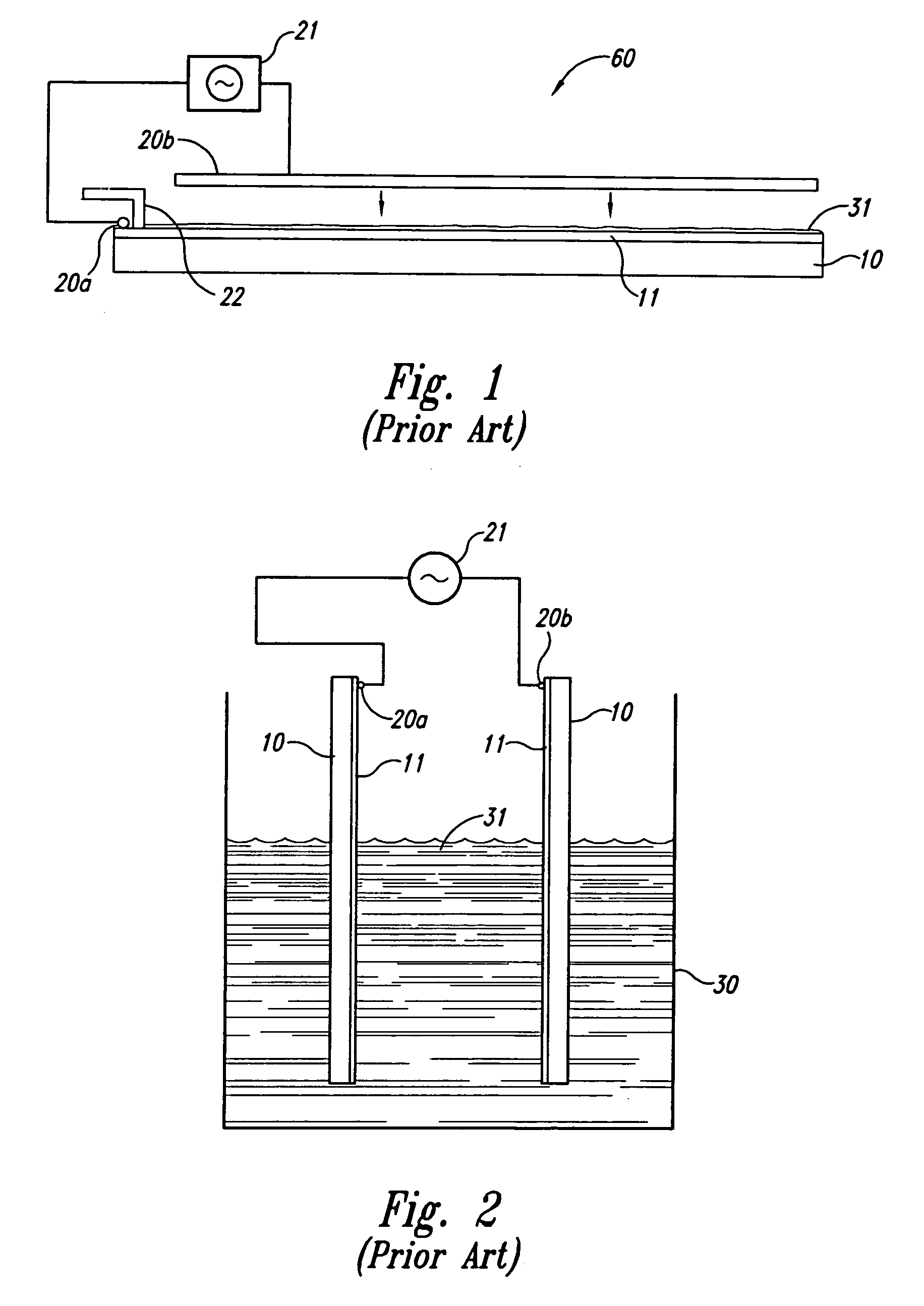
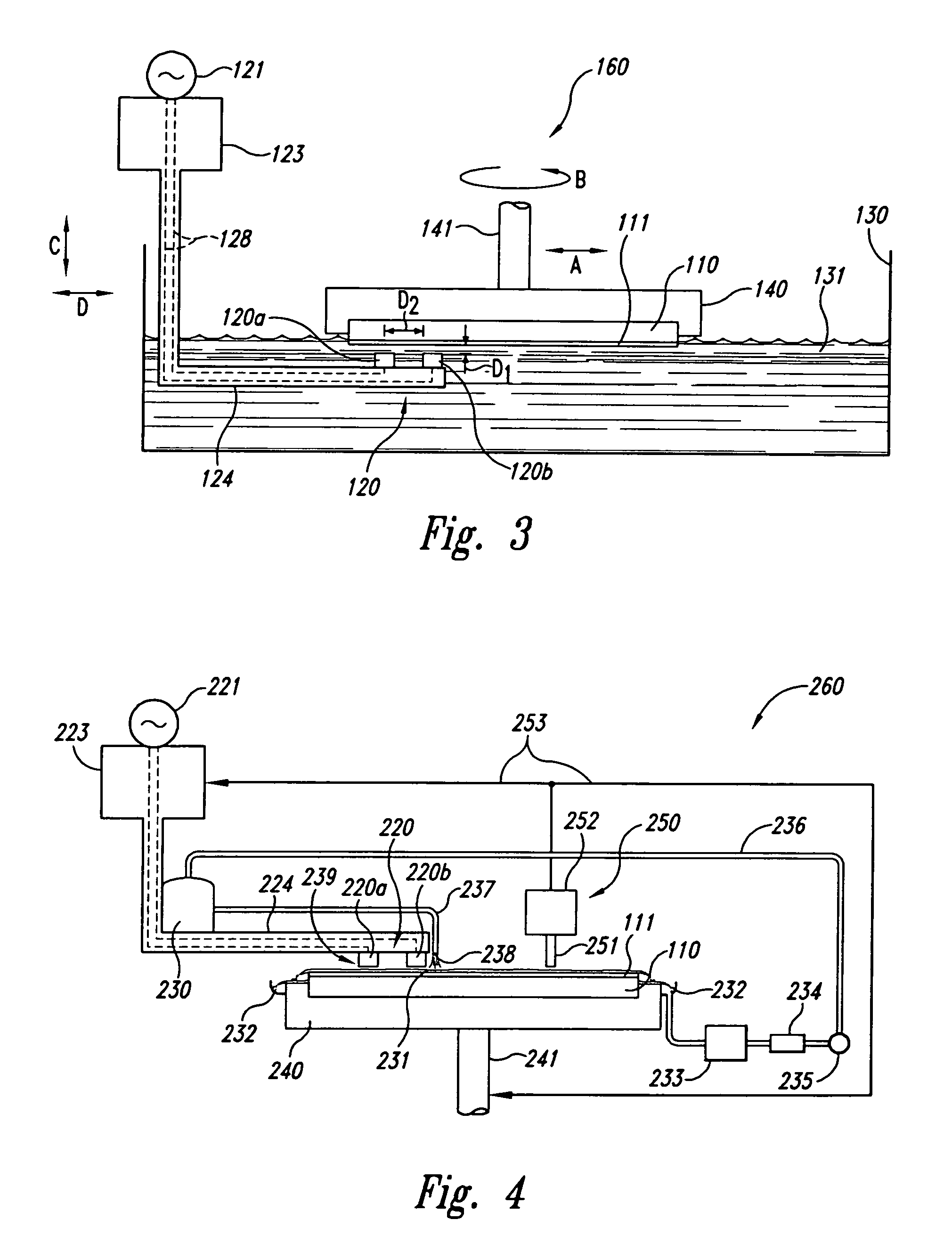
[0025]FIG. 3 is a partially schematic, side elevational view of an apparatus 160 for removing conductive material from a microelectronic substrate or substrate assembly 110 in accordance with an embodiment of the invention. In one aspect of this embodiment, the apparatus 160 includes a vessel 130 containing an electrolyte 131, which can be in a liquid or a gel state. A support member 140 supports the microele...


PUM

PropertyMeasurementUnit
Electrical conductivityaaaaaaaaaa
Flow rateaaaaaaaaaa
Currentaaaaaaaaaa

Abstract

A method and apparatus for removing conductive material from a microelectronic substrate. In one embodiment, a support member supports a microelectronic substrate relative to first and second electrodes, which are spaced apart from each other and spaced apart from the microelectronic substrate. One or more electrolytes are disposed between the electrodes and the microelectronic substrate to electrically link the electrodes to the microelectronic substrate. The electrodes are then coupled to a source of varying current that electrically removes the conductive material from the substrate. The microelectronic substrate and / or the electrodes can be moved relative to each other to position the electrodes relative to a selected portion of the microelectronic substrate, and the electrodes can be integrated with a planarizing portion of the apparatus to remove material from the conductive layer by chemical-mechanical planarization.

Description

TECHNICAL FIELD[0001]This invention relates to methods and apparatuses for removing conductive material from microelectronic substrates.BACKGROUND OF THE INVENTION[0002]Microelectronic substrates and substrate assemblies typically include a semiconductor material having features, such as memory cells, that are linked with conductive lines. The conductive lines can be formed by first forming trenches or other recesses in the semiconductor material, and then overlaying a conductive material (such as a metal) in the trenches. The conductive material is then selectively removed to leave conductive lines extending from one feature in the semiconductor material to another.[0003]Electrolytic techniques have been used to both deposit and remove metallic layers from semiconductor substrates. For example, an alternating current can be applied to a conductive layer via an intermediate electrolyte to remove portions of the layer. In one arrangement, shown in FIG. 1, a conventional apparatus 60 ...

Claims


Application Information

Patent Timeline
IPC IPC(8): B24B1/00B23H3/00B23H5/08B24B7/19H01L21/8242H01L29/00
CPCB23H5/08
Inventor MOORE, SCOTT E.
Owner MICRON TECH INC
Features
  • Generate Ideas
  • Intellectual Property
  • Life Sciences
  • Materials
  • Tech Scout
  • Unparalleled Data Quality
  • Higher Quality Content
  • 60% Fewer Hallucinations
Learn More