Electro-optical having a configuration to prevent generation and trapping of material residues

a technology of electro-optical material and configuration, applied in the direction of semiconductor devices, identification means, instruments, etc., can solve the problems of inability to cope with steps caused, and inability of related art technologies to cope with depressions generated on the surface of pixel electrodes, etc., to reduce or prevent damage, the effect of reducing or preventing an even

Active Publication Date: 2006-07-11
138 EAST LCD ADVANCEMENTS LTD
View PDF9 Cites 11 Cited by
  • Summary
  • Abstract
  • Description
  • Claims
  • Application Information

AI Technical Summary

Benefits of technology

[0015]In an aspect of the present invention, particularly, the protection insulating film is formed in the gaps between the pixel electrodes on at least part of the underlying layer and is also formed to lie on the edge portions of the pixel electrodes. Thus, the protection insulating film is provided so as to cover the end surfaces of edge portions of the pixel electrodes. Such a protection insulating film is provided, for example, by patterning a transparent insulating film containing silicon oxide, silicon nitride, or the like. The alignment layer is provided on a surface including the protection insulating film and the center portions of the pixel electrodes and is rubbed in a predetermined rubbing direction. Since the edges of the pixel electrodes are covered with the insulating film, the heights of steps in the vicinities of the pixel electrodes are reduced. Thus, the amount of material residues of the alignment layer which are generated in the vicinities of edges of the pixel electrodes during the rubbing process of the alignment layer containing polyimide or the like can be efficiently reduced. In addition, it is possible to effectively reduce or prevent an event that the edges of the pixel electrodes and the alignment layer provided thereon locally or microscopically peel off at the time of rubbing. As a result, material residues of the alignment layer which are generated in conjunction with the peeling off are also reduced. Further, rubbing failure that occurs in conjunction with the peeling-off can also be reduced consequently. In addition, for example, it is also possible to effectively reduce or prevent material residues generated as described above from being suspended in the electro-optic material, such as liquid crystal.
[0062]Since the electronic apparatus of an aspect of the present invention includes the electro-optical device of an aspect of the present invention, the electronic apparatus has reduced brightness irregularities and display irregularities. Thus, it is possible to achieve various electronic apparatuses that can display a high-quality image. Examples of such apparatuses include projection-type display apparatuses, liquid-crystal televisions, portable telephones, electronic organizers, word processors, viewfinder-type or monitor-direct-viewing-type videotape recorders, workstations, videophones, POS terminals, and touch panels. In addition, the electronic apparatus of an aspect of the present invention also can implement, for example, an electrophoresis apparatus for an electronic paper or the like.

Problems solved by technology

With this type of electro-optical device, when the substrate surface that faces the liquid crystal and the like has protrusions / depressions or steps, the operational state of the electro-optic material, such as the alignment state of the liquid crystal becomes unstable.
The related art technologies, however, cannot cope with steps caused by the presence of the pixel electrodes themselves.
In addition, these techniques typically cannot cope with depressions that are generated in the surfaces of the pixel electrodes so as to correspond to the openings of contact holes for directly or indirectly connecting the pixel electrodes to the thin-film transistors.
Further, the steps in the vicinities of the edges of such pixel electrodes or depressions in the vicinities of the contact holes cause polyimide residues or the like to be generated or trapped when the alignment layer formed of polyimide or the like on the pixel electrodes is rubbed.
The material residues from the alignment layer pose a technical problem in brightness irregularities or display irregularities occur in an image eventually displayed.
Thus, the technical problem due to such residues generated or trapped in the vicinities of the edges of the pixel electrodes or in the vicinities of the contact holes and due to residues suspended in the electro-optic material becomes more severe.

Method used


Image

  • Electro-optical having a configuration to prevent generation and trapping of material residues
  • Electro-optical having a configuration to prevent generation and trapping of material residues
  • Electro-optical having a configuration to prevent generation and trapping of material residues

Examples


Embodiment Construction

[0080]Embodiments of the present invention will be described below with reference to the accompanying figures. An exemplary embodiment described below is directed to a case in which an electro-optical device of an aspect of the present invention is applied to a TFT active-matrix-drive system liquid crystal device.

Configuration of Pixel Portion

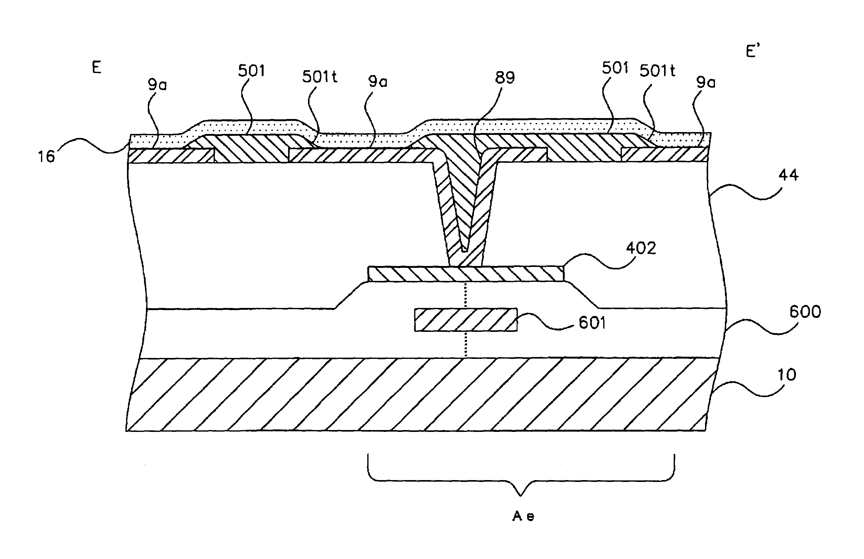
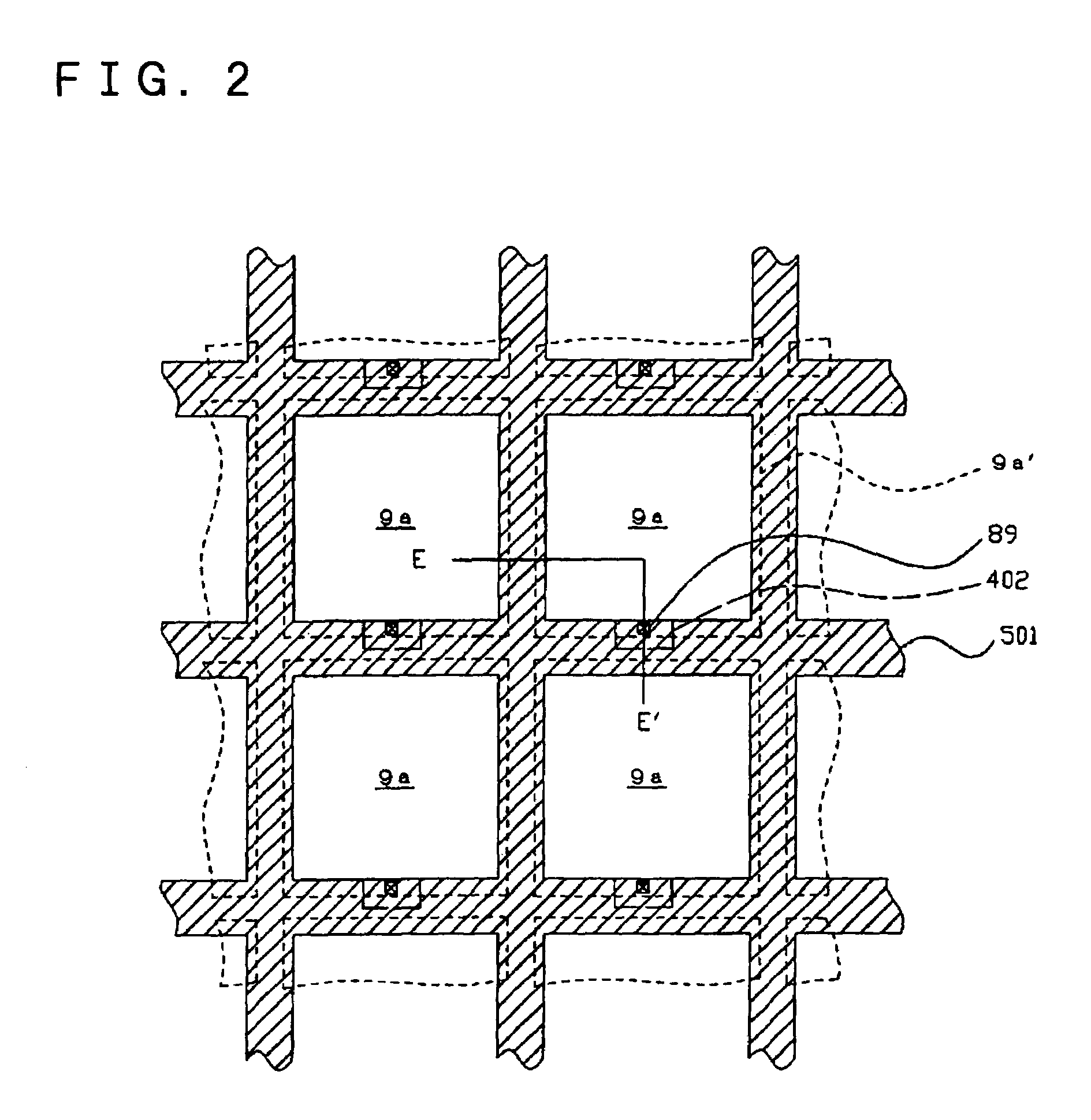
[0081]A pixel portion of an electro-optical device according to an exemplary embodiment of the present invention will be described with reference to FIGS. 1 to 7.

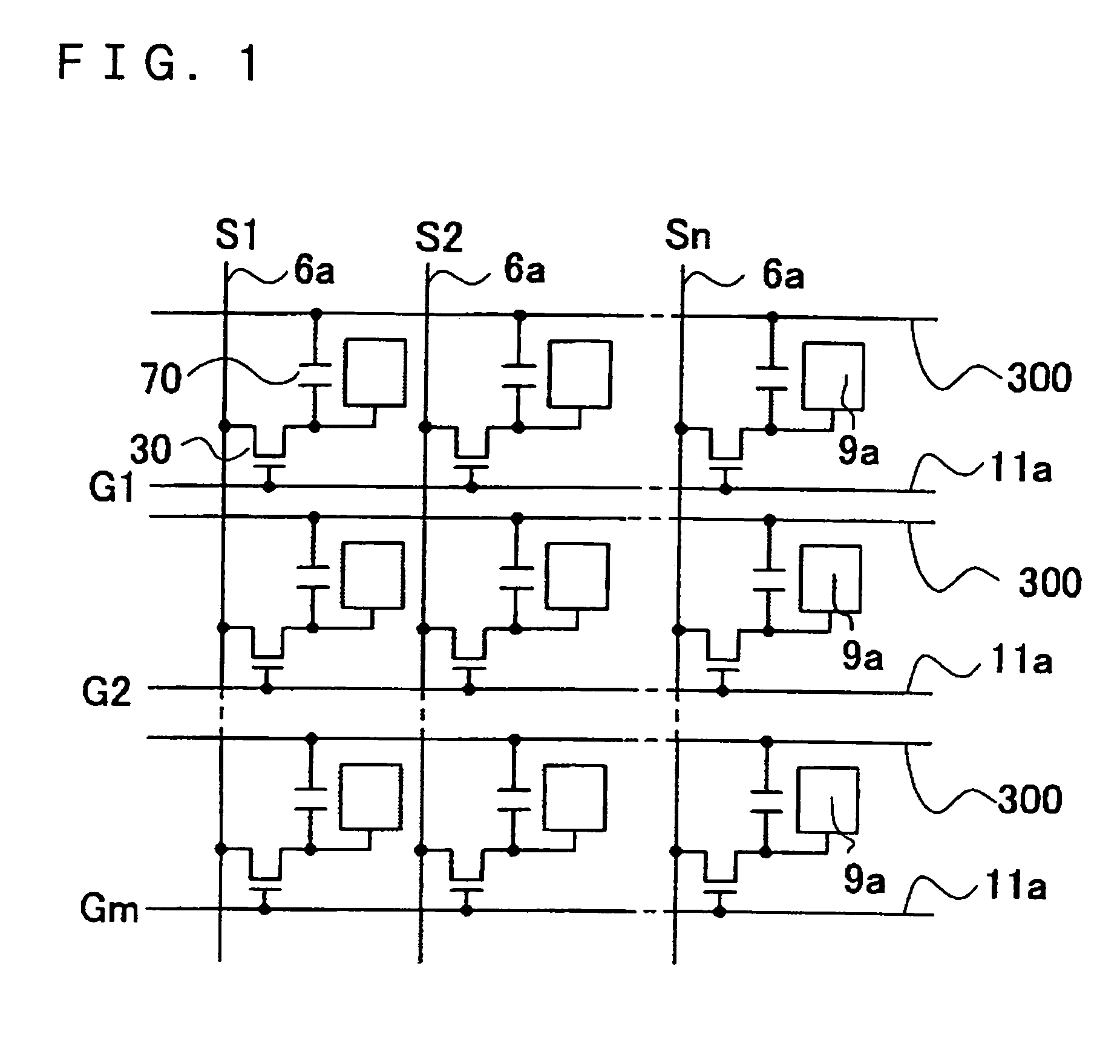
[0082]First, the electrical-circuit configuration thereof will be described with reference to FIG. 1. FIG. 1 is an equivalent circuit of various elements, wires, and the like for a plurality of pixels that are formed in a matrix to constitute an image display area of an electro-optical device.

[0083]Referring to FIG. 1, the plurality of pixels, which are formed in a matrix to constitute the image display area of the electro-optical device of the present exemplary embodiment, have corres...


PUM

PropertyMeasurementUnit
taper angleaaaaaaaaaa
thicknessaaaaaaaaaa

Abstract

An electro-optical device for a liquid-crystal apparatus includes TFTs provided above a substrate, pixel electrodes that are provided above the TFTs and that are connected to corresponding relay electrodes via contact holes, a protection insulating film that is provided on the pixel electrodes from the gaps between the pixel electrodes to the edge portions thereof so as to cover end surfaces of the edge portions of the pixel electrodes, and an alignment layer that is provided on a surface including the protection insulating film and that is rubbed. Material residues of the alignment layer are reduced or prevented from being generated or trapped in the vicinities of the edges of the pixel electrodes and in the vicinities of the contact holes. Consequently, brightness irregularities or display irregularities are reduced.

Description

BACKGROUND OF THE INVENTION[0001]1. Field of Invention[0002]The present invention relates to a technical field of an electro-optical device, such as a liquid crystal device, a manufacturing method therefor, and an electronic apparatus, such as a liquid crystal projector having the electro-optical device.[0003]2. Description of Related Art[0004]In general, an electro-optical device has a configuration in which electro-optic material, such as liquid crystal, is sandwiched between a pair of substrates, above one of which, pixel electrodes for pixels are provided so as to face the liquid crystal. In this case, the pixel electrodes are arranged in a matrix at a constant pitch (hereinafter referred to as “a pixel pitch” as appropriate). The surfaces of the pixel electrodes or the substrate surface that is in contact with the liquid crystal and the like are provided with an alignment layer for defining the operational state of the electro-optic material, such as the alignment state of the ...

Claims


Application Information

Patent Timeline
Patent Type & Authority Patents(United States)
IPC IPC(8): H01L29/04H01L31/20H01L31/036H01L31/0376G02F1/1333G02F1/1335G02F1/1337G02F1/1343G02F1/1362G02F1/1368G09F9/00G09F9/30H01L27/12
CPCG02F1/136227H01L27/12G02F2001/133357G02F1/133357G02F1/1337
Inventor TAKAHARA, KENICHI
Owner 138 EAST LCD ADVANCEMENTS LTD
Why Eureka
Try Eureka