Method for forming leadless semiconductor packages

Active Publication Date: 2006-08-08
ADVANCED SEMICON ENG INC
View PDF1 Cites 78 Cited by
  • Summary
  • Abstract
  • Description
  • Claims
  • Application Information

AI Technical Summary

Benefits of technology

[0011]The present invention utilizes an etching process to remove interval regions and outer dambars of a leadframe to expose a metal layer, and then utilizes a half cutting process to cut off the metal layer located in the interval regions and a singulation process to singulate units of the leadframe by cutting

Problems solved by technology

However, the conventional leadframe package possesses rather long outer leads and inner leads, and it is gradually unable to satisfy the development of the integrated circuits, which have high numbers of input/output

Method used


Image

  • Method for forming leadless semiconductor packages
  • Method for forming leadless semiconductor packages
  • Method for forming leadless semiconductor packages

Examples


Embodiment Construction

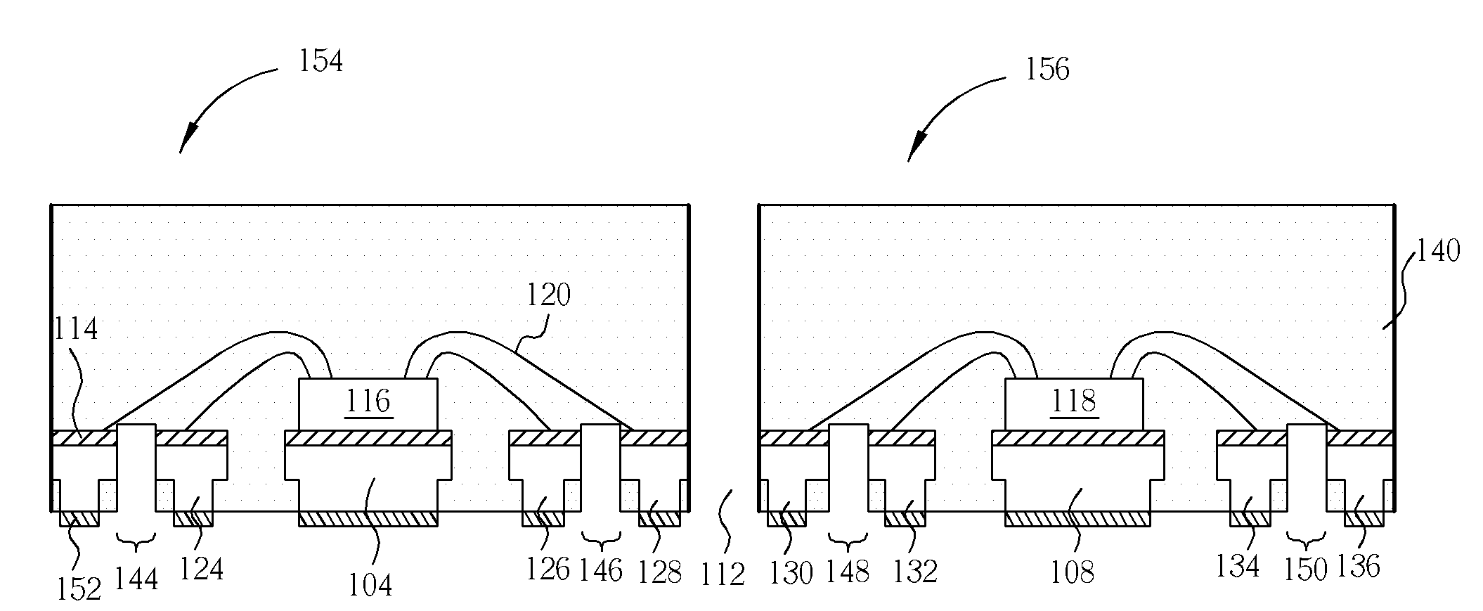
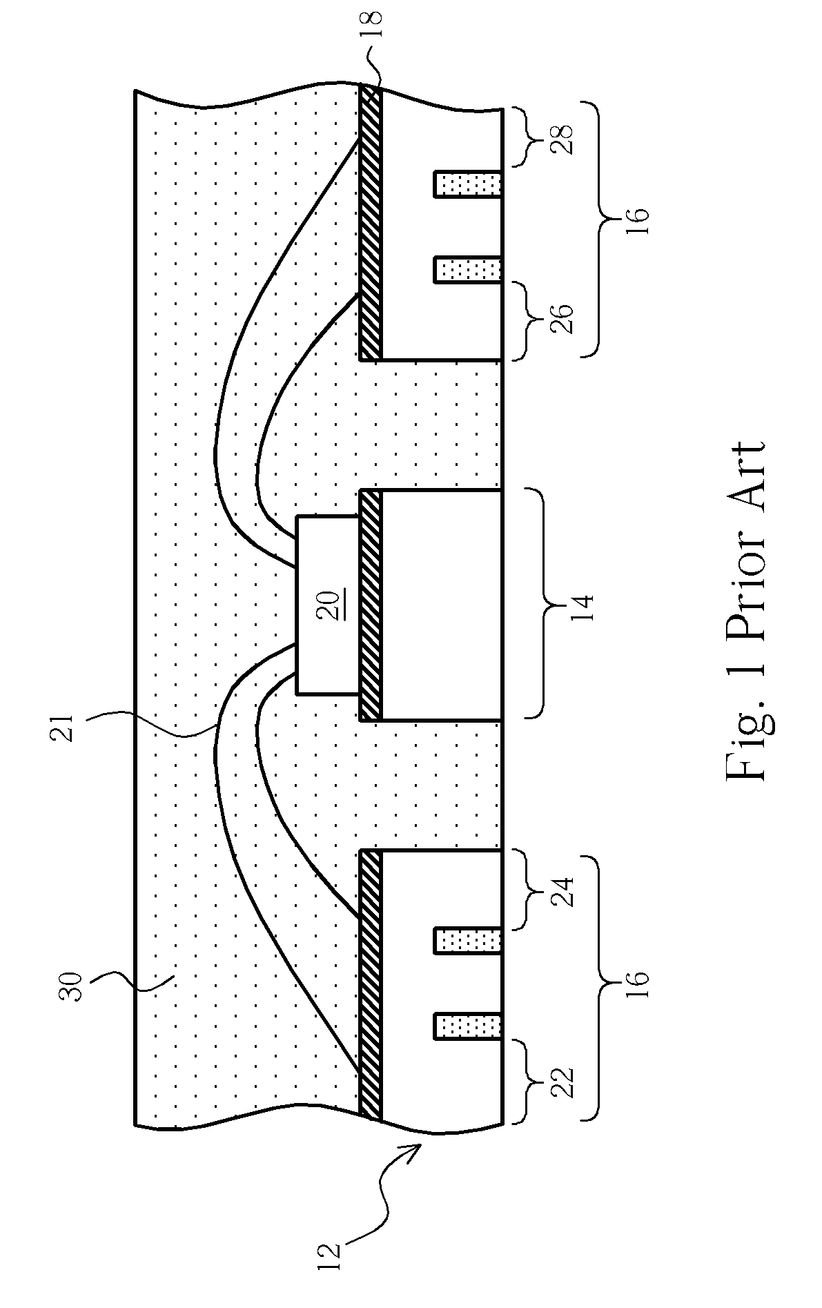
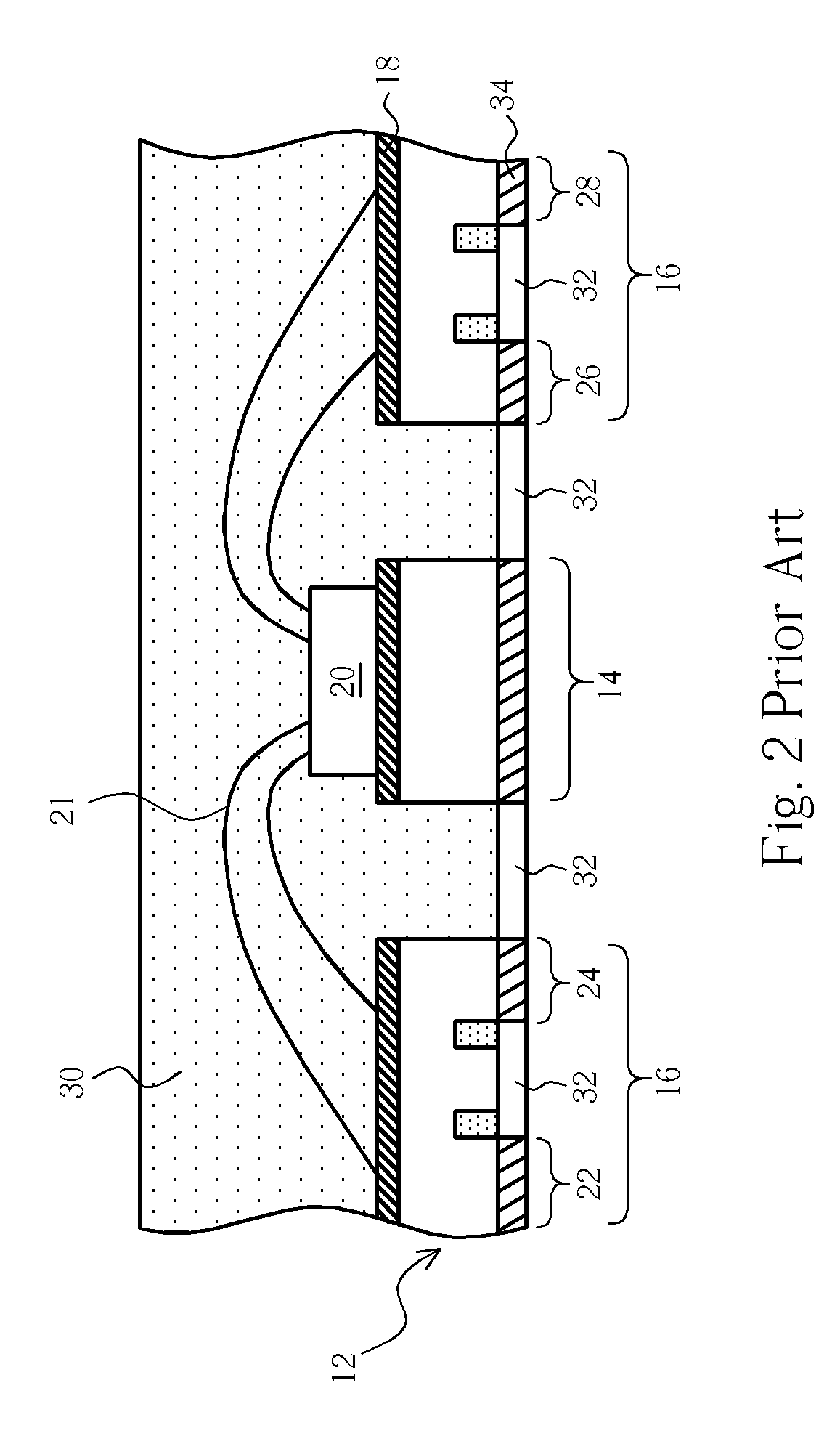
[0017]The present invention provides a method for forming leadless semiconductor packages, and it applies to each kind of leadframes such as in-line lead leadframes and staggered lead leadframes shown in FIG. 4. FIG. 4 is a schematic diagram showing a plurality of leadframes 40, 42, 44, 46, 48, and 50. In general, a leadframe usually includes a plurality of units in an array arrangement. However, the leadframes shown in FIG. 4 are merely exemplary embodiments, and a unit is represented by each of the leadframes. As shown in FIG. 4, a leadframe 40 includes a die pad 52, a plurality of staggered leads 54, a plurality of tie bars 56, and a plurality of outer dambars 58. The tie bars 56 connect the die pad 52 and the outer dambars 58, and the leads 54 connect to the outer dambars 58. A leadframe 42 includes a die pad 60, a plurality of in-line leads 62, a plurality of tie bars 64, and a plurality of outer dambars 66. The tie bars 64 connect the die pad 60 and the outer dambars 66, and t...


PUM


Abstract

The present invention includes providing a leadframe including a metal layer formed on an upper surface of the leadframe and a plurality of units in an array arrangement, in which each unit includes a die pad, a plurality of leads, and a plurality of outer dambars, adhering a die to the die pad, forming a plurality of conductive wires to electrically connect bond pads of the die with bond regions of the leads, forming an encapsulation covering the leadframe, forming a patterned photoresist layer on a lower surface of the leadframe to expose a plurality of interval regions and the outer dambars, performing an etching process to expose the metal layer located in the interval regions and the outer dambars, cutting off the metal layer located in the interval regions by a half cutting process, and performing a singulation process to singulate the units.

Description

BACKGROUND OF THE INVENTION[0001]1. Field of the Invention[0002]The present invention relates to a method for forming leadless semiconductor packages, and more particular, to a method for forming leadless semiconductor packages which is capable of reducing the number of saw blades used.[0003]2. Description of the Prior Art[0004]The conventional leadframe package has been applied widely for a long time in the integrated circuit package field. It has advantages such as low manufacturing cost, high reliability, and so forth. However, the conventional leadframe package possesses rather long outer leads and inner leads, and it is gradually unable to satisfy the development of the integrated circuits, which have high numbers of input / output (I / O) connections and tiny sizes. For this reason, a leadless semiconductor package is developed and applied gradually. Since it is leadless, it is capable of reducing the footprint and the package size. Moreover, since the length of the lead is shorte...

Claims


Application Information

Patent Timeline
IPC IPC(8): H01L21/44
CPCH01L21/561H01L23/3107H01L23/49548H01L23/49582H01L24/48H01L24/97H01L2924/01033H01L2924/00014H01L2924/30107H01L2924/14H01L2924/01082H01L2924/01078H01L2924/0105H01L2924/01047H01L2924/01029H01L2224/97H01L2224/85439H01L2221/68377H01L2224/05599H01L2224/48091H01L2224/48247H01L2224/484H01L2224/85399H01L2224/85H01L2224/45099H01L2924/181H01L2924/18301H01L2924/00012
Inventor PARK, SANG-BAELEE, YONG-GILLPARK, HYUNG-JUNSOHN, CHANG-YOUNG
Owner ADVANCED SEMICON ENG INC
Why Eureka
Try Eureka