Unlock instant, AI-driven research and patent intelligence for your innovation.

Method for generating chip stacks

a technology of chip contacting device and chip, which is applied in the direction of individual semiconductor device testing, semiconductor/solid-state device testing/measurement, instruments, etc., can solve the problems of not having the positioning accuracy of chips, the use of chip serial process is very time-consuming, and the chip contacting device not having a sufficient positioning accuracy does not achieve the output required for a production

Active Publication Date: 2006-08-08
DISCO HI TEC EURO +1
View PDF11 Cites 10 Cited by
  • Summary
  • Abstract
  • Description
  • Claims
  • Application Information

AI Technical Summary

Benefits of technology

This approach achieves high output with precise positioning accuracy, ensures all chip stacks are composed of good chips, and allows for efficient exchange of defective chips without reducing yield, enabling effective throughplating.

Problems solved by technology

The drawback of this procedure is that for assembling the chips a serial process is used which is very time-consuming.
The chip contacting devices (diebonder) used for this process step—if they have an output suitable for production—do not have the positioning accuracy of the chips necessary for the subsequent throughplating.
On the other hand, chip contacting devices having a sufficient positioning accuracy do not achieve the output required for a production.
Consequently, it is not possible in a satisfying way to pick up the individual good chips and stack them during running production.
A drawback of this procedure is that although the yield with regard to the wafers used is good, the number of faultless chip stacks is accordingly low.
The drawback of this procedure is that during unmatching the position of the chips on the carrier foil changes.
The chip stacks thus may not have the positioning accuracy necessary for a subsequent throughplating.

Method used


Image

  • Method for generating chip stacks
  • Method for generating chip stacks
  • Method for generating chip stacks

Examples


Embodiment Construction

[0025]For the purposes of promoting an understanding of the principles of the present inventions, reference will now be made to the embodiments, or examples, illustrated in the drawings and specific language will be used to describe the same. It will nevertheless be understood that no limitation of the scope of the invention is thereby intended. Any alterations and further modifications in the described embodiments, and any further applications of the principles of the inventions as described herein are contemplated as would normally occur to one skilled in the art to which the invention relates.

[0026]For the most part, details unnecessary to obtain a complete understanding of the present invention have been omitted inasmuch as such details are within the skills of persons of ordinary skill in the relevant art.

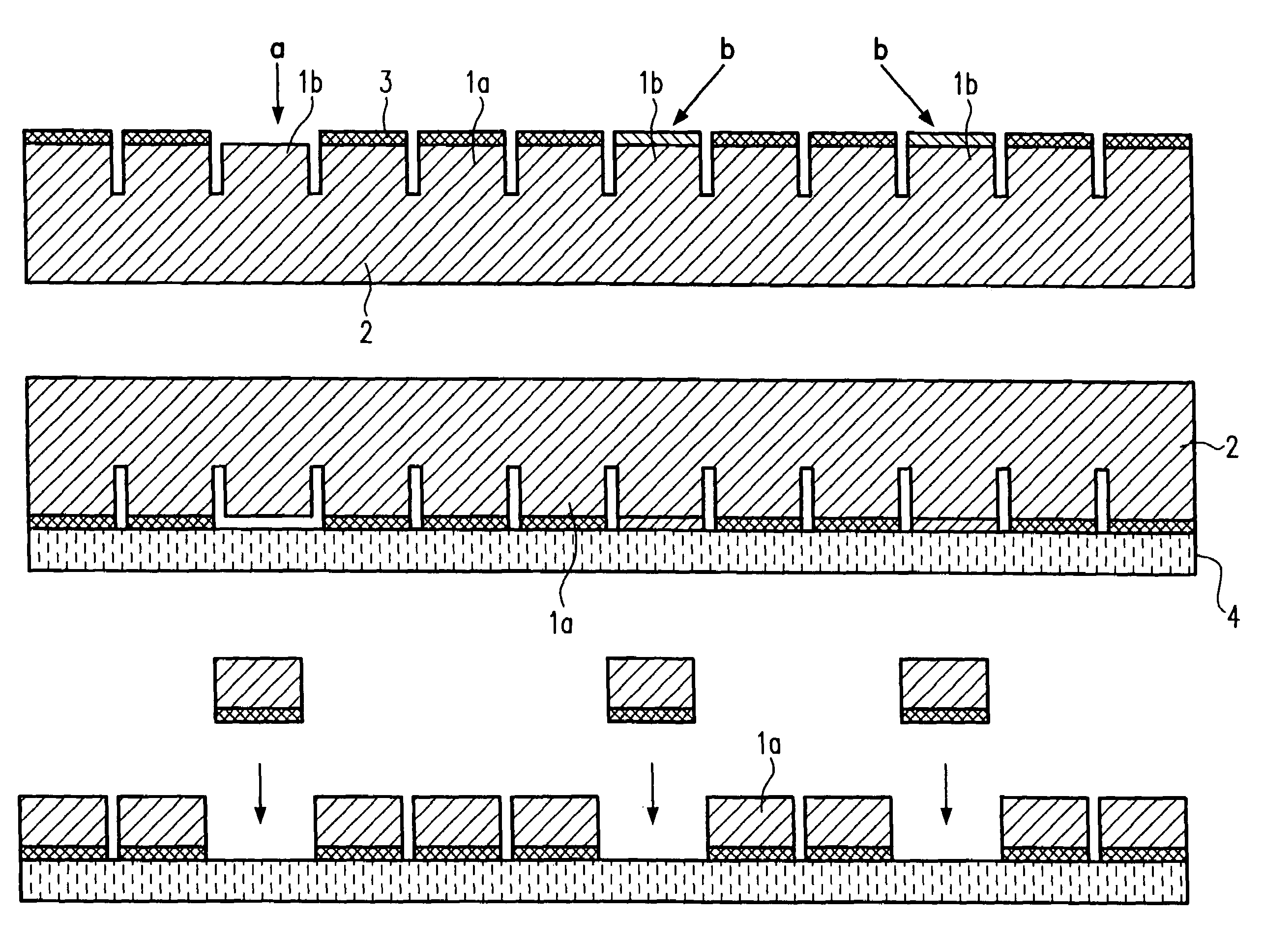
[0027]With reference to FIG. 6, it is known to lay unmatched chips down on a carrier or a carrier foil 4 which may be provided with a frame 5. As can be seen from the drawing,...


PUM


Abstract

Disclosed is a method for generating chip stacks during the production of chips from wafers, the chips located on the wafer being separated from one another, the wafer being ground thin and the chips being stacked to form chip stacks, the chips being checked for the purpose of a functional check, characterized in that the chips are checked in a first work step, that adhesive material is applied on the good chips, whereas the bad chips are not provided with adhesive material, that the wafer is assembled and ground thin afterwards and that the bad chips are subsequently removed and replaced by good chips.

Description

CROSS REFERENCE TO RELATED APPLICATIONS[0001]This application claims the benefit of the filing date of German patent application 10342980.8, entitled “Method for Generating Chip Stacks,” filed on Sep. 17, 2003, the disclosure of which is incorporated herein by reference.TECHNICAL FIELD[0002]Aspects of this invention relate in general to a method for generating chip stacks. In particular, aspects of the invention relate to a method for generating chip stacks during the production of chips from wafers, the chips located on the wafer being separated from one another, the wafer being ground thin and the chips being stacked to form chip stacks, the individual chips being subjected to a functional check in the course of the method.BACKGROUND INFORMATION[0003]During the production and further processing of chips, chip stacks are generated in order to increase the component density of the components. Such chip stacks (3D packages) are to include only functional chips (good chips).[0004]It i...

Claims


Application Information

Patent Timeline
Patent Type & Authority Patents(United States)
IPC IPC(8): H01L21/46H01L21/301H01L21/78H01L21/68H01L25/065
CPCH01L21/6835H01L21/6836H01L21/78H01L25/50H01L24/27H01L25/0657H01L2221/68327Y10S438/977H01L2224/274H01L2224/83191H01L2225/06513H01L2924/01019H01L2221/6834
Inventor PRIEWASSER, KARL HEINZWINTER, SYLVIA
Owner DISCO HI TEC EURO