
Method for driving liquid crystal display device

Inactive Publication Date: 2006-08-08
SEMICON ENERGY LAB CO LTD
View PDF12 Cites 4 Cited by
  • Summary
  • Abstract
  • Description
  • Claims
  • Application Information

AI Technical Summary

Benefits of technology

[0015]Thus, the present invention has been achieved in view of the above-mentioned problems; the invention realizes a liquid crystal display device in which the deterioration of the image due to image persistence can be prevented.
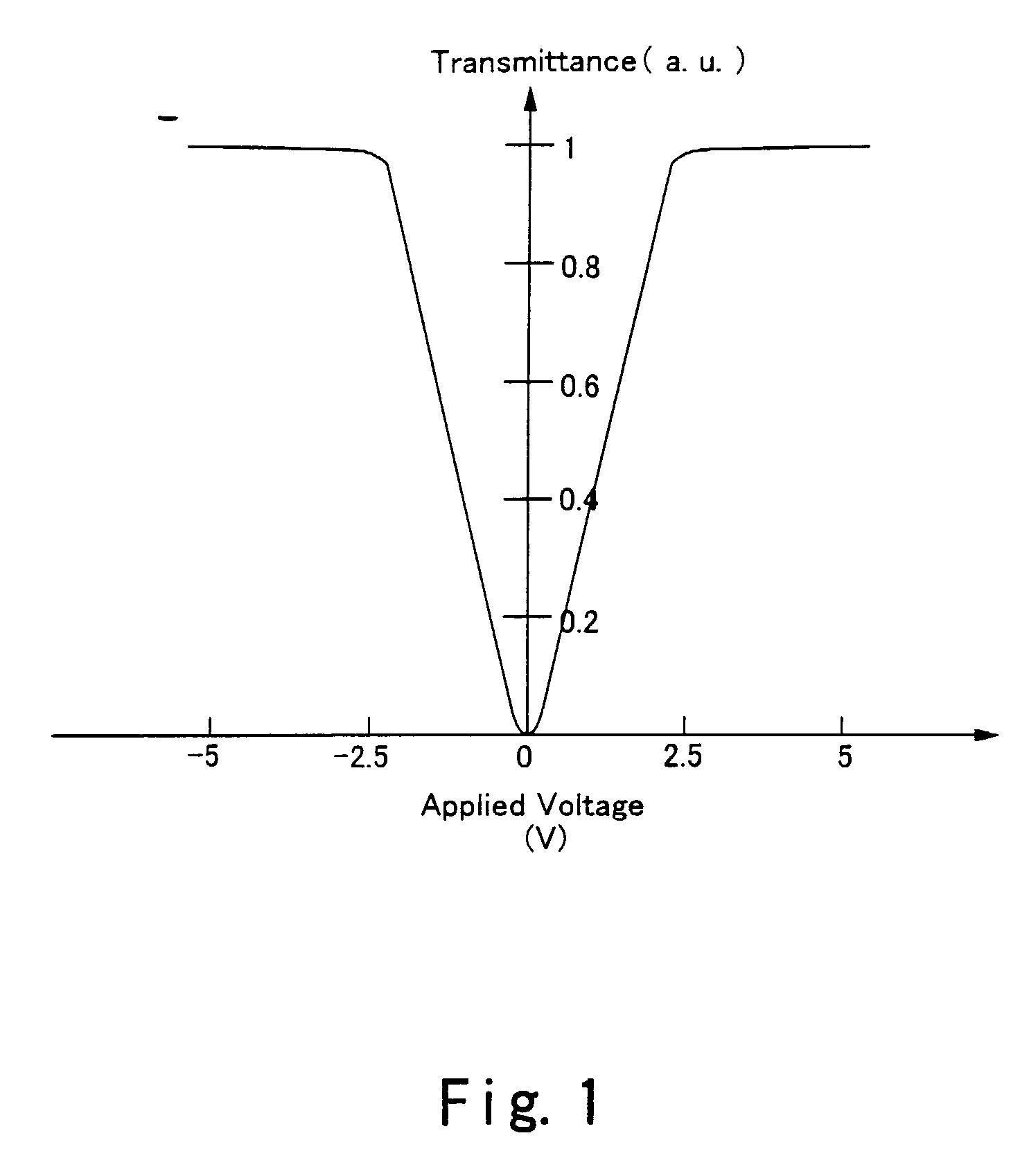
[0064]In the case of using a thresholdless antiferrorelectric mixed liquid as shown in FIG. 1, high-speed driving, low-voltage driving and gradation display become possible.
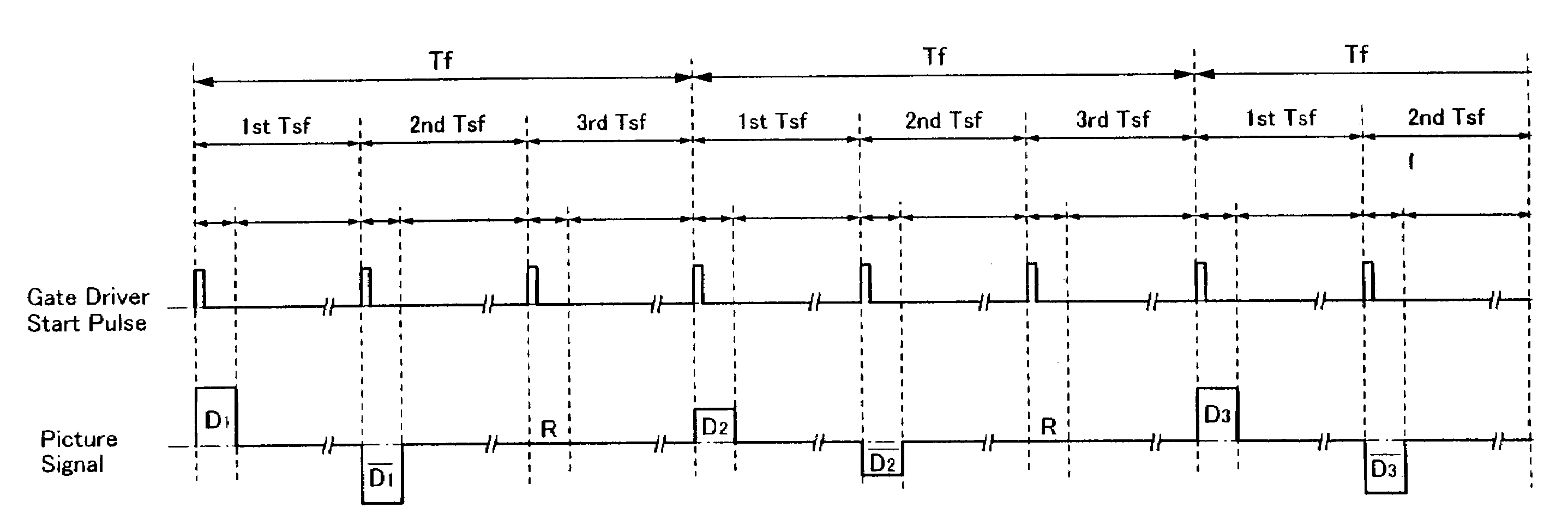
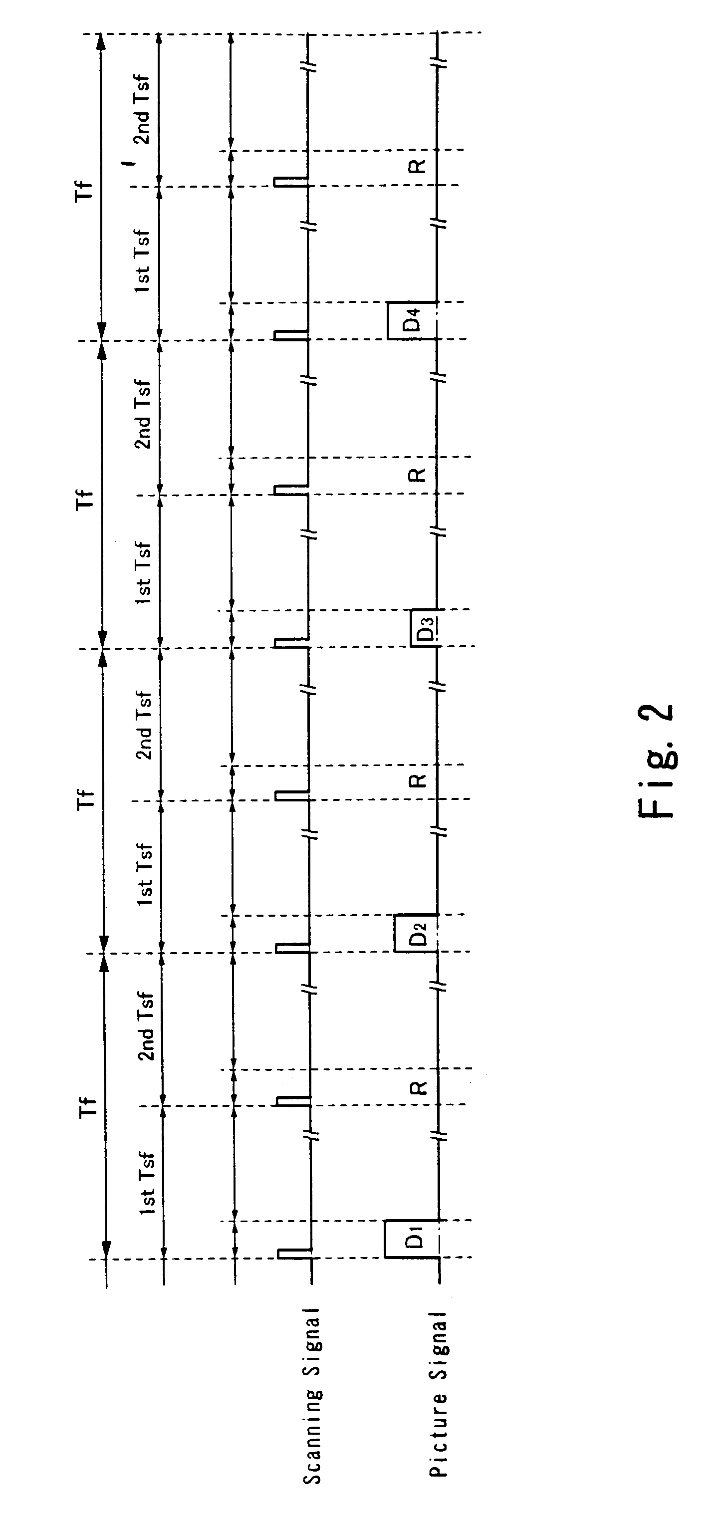
[0071]In this way, in the above-mentioned liquid crystal display device according to the present invention, the display of black is performed during one of the two sub-frames constituting one frame, so that image persistence can be prevented.
[0078]As mentioned above, in the liquid crystal display device according to the invention, during at least one of a plurality of sub-frames constituting one frame, a reset signal is fed to perform the display of black, so that the occurrence of image persistence can be prevented.

Problems solved by technology

Further, in the case of realizing the screen enlargement of the matrix liquid crystal display device and rendering the matrix liquid crystal display device highly precise and minute, the TN mode (twist nematic mode) using the known nematic liquid crystal cannot be said to be sufficient in its response speed.
However, in the case this antiferroelectric mixed liquid crystal with a V-shaped electrooptical characteristic is used in an active matrix liquid crystal display device, the “image persistence” is more apt to take place than in the case of using nematic liquid crystal, thus leading to the problem of image deterioration.

Method used


Image

  • Method for driving liquid crystal display device
  • Method for driving liquid crystal display device
  • Method for driving liquid crystal display device

Examples


embodiment 1

[0109]FIG. 4 will now be referred to. FIG. 4 shows an outline of the constitution of the liquid crystal display device according to this embodiment. The reference numeral 101 denotes a liquid crystal display device that has digital drivers. The liquid crystal display device 101 includes an active matrix substrate 101-1 and an opposite substrate 101-2 (not shown). The active matrix substrate 101-1 includes a source driver 101-1-1, a gate driver 101-1-2, a digital video data division circuit 101-1-3 and a pixel portion 101-1-4 in which a plurality of pixel TFTs are matrix-wise disposed. The source driver 101-1-1 and the gate driver 101-1-2 drive a plurality of the pixels in the pixel portion. Further, the opposite substrate 101-2 includes an opposite electrode 101-2-1 (not shown). Numerals 103-1 and 103-2 denote FPC (Flexible Print Circuit) terminals; and, to these FPC terminals, various signals are inputted from the outside.

[0110]Next, FIG. 5 will be referred to. FIG. 5 is a diagram ...

embodiment 2

[0145]This embodiment relates to the liquid crystal display device of the present invention based on a display method different from the above-mentioned display method of Embodiment 1. The constitution of the liquid crystal display device according to this embodiment is identical with that of Embodiment 1, so that reference can be made to Embodiment 1.

[0146]The display method of the liquid crystal display device according to this embodiment will be described. FIG. 9 will now be referred to. FIG. 9 shows a driving timing chart of the liquid crystal display device according to this embodiment. In the liquid crystal display device of the present invention, which will be described here, one frame is formed of four sub-frames. Here, one frame period (Tf) is constituted of a first sub-frame period (1st Tsf), a second sub-frame period (2nd Tsf), a third sub-frame period (3rd Tsf) and a fourth sub-frame period (4th Tsf).

[0147]In FIG. 9, the pixel P1,1, the pixel P2,1 and the pixel P1079,1 a...

embodiment 3

[0155]FIG. 10 will now be referred to. FIG. 10 is a diagram showing an outline of the constitution of the liquid crystal display device according to this embodiment. Numeral 1001 denotes a liquid crystal display device that has digital drivers. The liquid crystal display device 1001 includes an active matrix substrate 1001-1 and an opposite substrate 1001-2 (not shown). The active matrix substrate 1001-1 includes a source driver 1001-1-1, a source driver 1001-1-2, a gate driver 1001-1-3, a digital video data division circuit 1001-1-4 and a pixel portion 1001-1-5 in which a plurality of pixel TFTs are matrix-wise disposed. The source driver 1001-1-1, the source driver 1001-1-2 and the gate driver 1001-1-3 drive a plurality of the pixel TFTs in the pixel portion. Further, the opposite substrate 1001-2 includes an opposite electrode 1001-2-1 (not shown). Numerals 1003-1 and 1003-2 denote FPC terminals; to these FPC terminals, various signals are inputted from the outside.

[0156]The sour...


PUM


Abstract

A liquid crystal display device afflicted with no image persistence is disclosed. The liquid crystal display device according to the present invention comprises a pixel portion in which a plurality of pixel TFTs are matrix-wise disposed, a source driver and a gate driver which feed a plurality of the TFTs with picture signals, and a liquid crystal material which has substantially no threshold value, characterized in that one frame is formed of a plurality of sub-frames, and, during at least one of a plurality of the sub-frames, the display by a reset signal is performed.

Description

[0001]This is a continuation of Ser. No. 09 / 570,698 filed May 12, 2000 now U.S. Pat. No. 6,545,656.BACKGROUND OF THE INVENTION[0002]1. Field of the Invention[0003]The present invention relates to a liquid crystal display device. The invention also relates to electrooptical apparatus using the liquid crystal display device.[0004]2. Description of the Prior Art[0005]Recently, the technique of fabricating thin film transistors (TFTs) on cheap glass substrates is being rapidly developed. The reason therefore lies in that the demand for active matrix liquid crystal display devices is increasing.[0006]An active matrix liquid crystal display device is constituted in such a manner that a pixel portion is comprised of several hundred thousands to several millions of pixels which are matrix-wise disposed, a pixel TFT is disposed in each of the pixels, and the charges entering and leaving the pixel electrode connected to each pixel TFT are controlled by the switching function of the pixel TFT....

Claims


Application Information

Patent Timeline
IPC IPC(8): G09G3/36G09G3/20
CPCG09G3/3651G09G3/3648G02F1/13454G09G3/2022G09G3/3614G09G2320/0252G09G2310/027G09G2310/061
Inventor YAMAZAKI, SHUNPEI
Owner SEMICON ENERGY LAB CO LTD
Learn More