

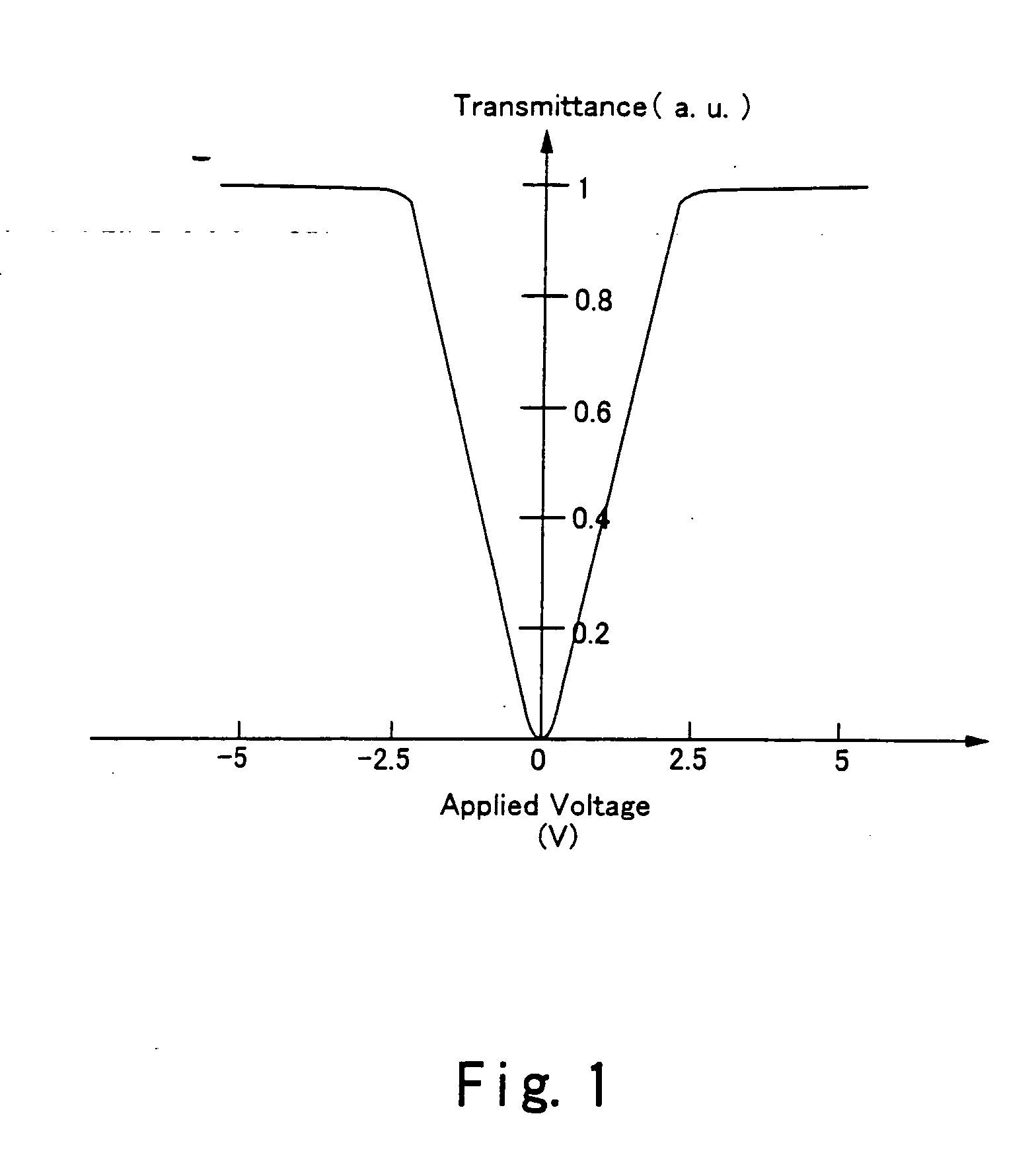
Liquid crystal display device
a liquid crystal display and display device technology, applied in static indicating devices, non-linear optics, instruments, etc., can solve the problems of image deterioration, insufficient response speed of tn mode using the known nematic liquid crystal, etc., and achieve the effect of preventing image deterioration due to image persisten
- Summary
- Abstract
- Description
- Claims
- Application Information
AI Technical Summary
Benefits of technology
Problems solved by technology
Method used
Image

Examples
embodiment 1
[0108]FIG. 4 will now be referred to. FIG. 4 shows an outline of the constitution of the liquid crystal display device according to this embodiment. The reference numeral 101 denotes a liquid crystal display device that has digital drivers. The liquid crystal display device 101 includes an active matrix substrate 101-1 and an opposite substrate 101-2 (not shown). The active matrix substrate 101-1 includes a source driver 101-1-1, a gate driver 101-1-2, a digital video data division circuit 101-1-3 and a pixel portion 101-1-4 in which a plurality of pixel TFTs are matrix-wise disposed. The source driver 101-1-1 and the gate driver 101-1-2 drive a plurality of the pixels in the pixel portion. Further, the opposite substrate 101-2 includes an opposite electrode 101-2-1 (not shown). Numerals 103-1 and 103-2 denote FPC (Flexible Print Circuit) 1 terminals; and, to these FPC terminals, various signals are inputted from the outside.
[0109] Next, FIG. 5 will be referred to. FIG. 5 is a diag...
embodiment 2
[0144] This embodiment relates to the liquid crystal display device of the present invention based on a display method different from the above-mentioned display method of Embodiment 1. The constitution of the liquid crystal display device according to this embodiment is identical with that of Embodiment 1, so that reference can be made to Embodiment 1.
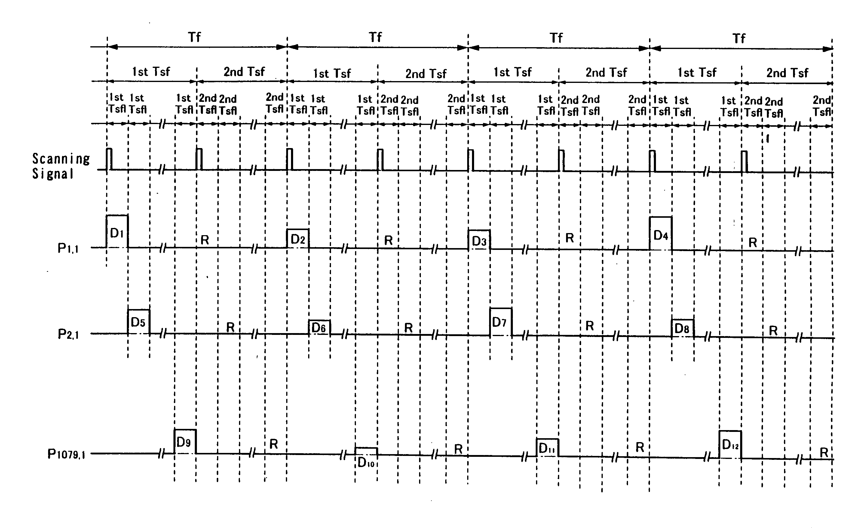
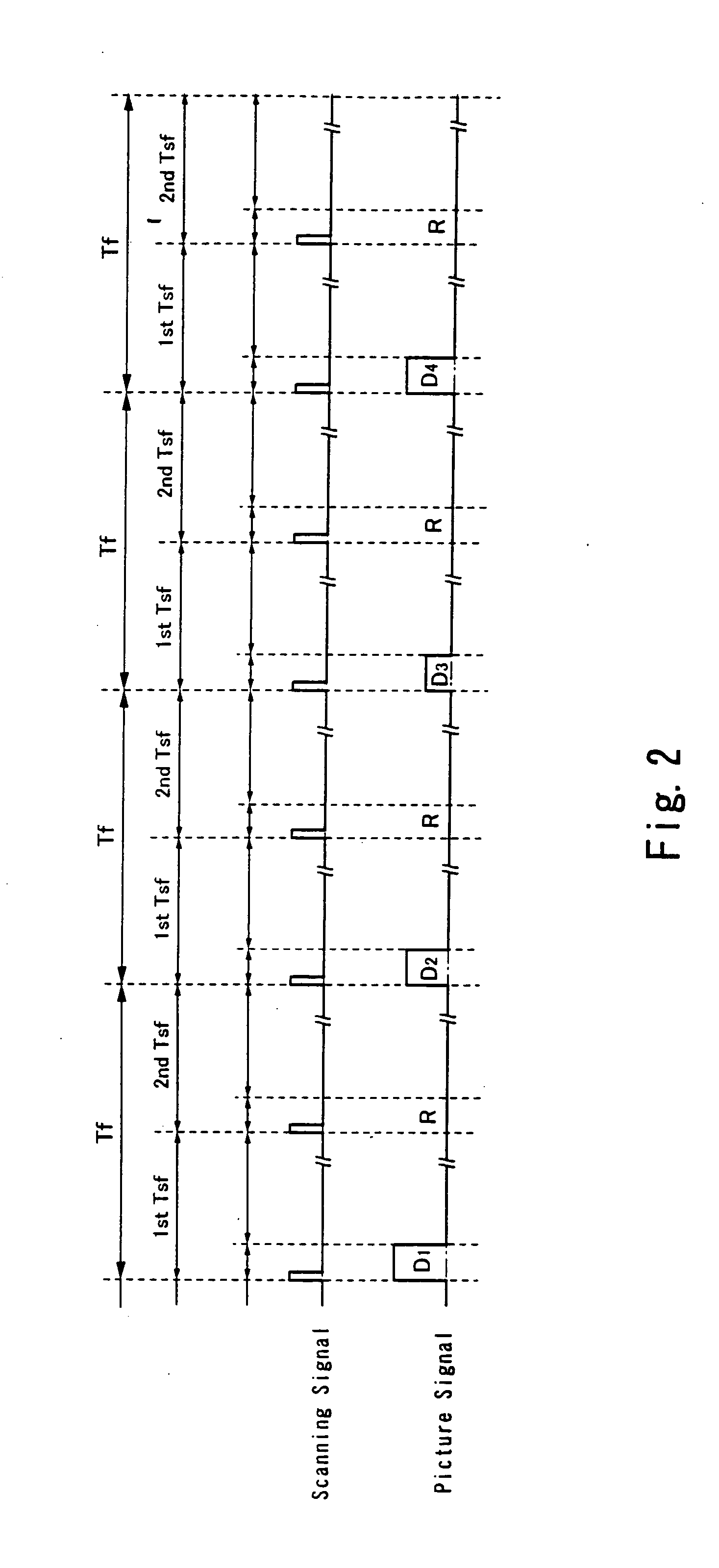
[0145] The display method of the liquid crystal display device according to this embodiment will be described. FIG. 9 will now be referred to. FIG. 9 shows a driving timing chart of the liquid crystal display device according to this embodiment. In the liquid crystal display device of the present invention which will be described here, one frame is formed of four sub-frames. Here, one frame period (Tf) is constituted of a first sub-frame period (1st Tsf), a second sub-frame period (2nd Tsf), a third sub-frame period (3rd Tsf) and a fourth sub-frame period (4th Tsf).
[0146] In FIG. 9, the pixel P1,1, the pixel P2,1 and the pixel P1079...
embodiment 3
[0154]FIG. 10 will now be referred to. FIG. 10 is a diagram showing an outline of the constitution of the liquid crystal display device according to this embodiment. Numeral 1001 denotes a liquid crystal display device that has digital drivers. The liquid crystal display device 1001 includes an active matrix substrate 1001-1 and an opposite substrate 1001-2 (not shown). The active matrix substrate 1001-1 includes a source driver 1001-1-1, a source driver m 1001-1-2, a gate driver 1001-1-3, a digital video data division circuit 1001-1-4 and a pixel portion 1001-1-5 in which a plurality of pixel TFTs are matrix-wise disposed. The source driver 1001-1-1, the source driver 1001-1-2 and the gate driver 1001-1-3 drive a plurality of the pixel TFTs in the pixel portion. Further, the opposite substrate 1001-2 includes an opposite electrode 1001-2-1 (not shown). Numerals 1003-1 and 1003-2 denote FPC terminals; to these FPC terminals, various signals are inputted from the outside.
[0155] The ...
PUM
 Abstract
Description
Claims
Application Information