Color display device

a display device and color technology, applied in the field of display devices, can solve the problems of light emission, complex circuitry, and complex arrangement of power source lines, and achieve the effect of easy control of white balance among display pixels for different colors

Inactive Publication Date: 2006-08-15
SANYO ELECTRIC CO LTD
View PDF24 Cites 59 Cited by
  • Summary
  • Abstract
  • Description
  • Claims
  • Application Information

AI Technical Summary

Benefits of technology

[0021]The object of the present invention is to provide an EL display device in which the sizes of the EL element driving TFTs in display pixels having EL elements for different colors are varied depending on emissive efficiency, such that the white balance among the display pixels for different colors can easily be controlled without requiring complex circuitry.

Problems solved by technology

This light radiates outward through the transparent anode via the transparent insulating substrate, resulting in light emission.
However, conventional display devices are disadvantageous in that, to alter the current value of the power source for each color of the display pixels, the power source line must be arranged in a complex manner within the region in which the display pixels are arranged.
Further, to alter the potential of the drain signal supplied to the first TFT according to each color, complex circuitry is necessary for supplying a signal to the first TFT.

Method used


Image

  • Color display device
  • Color display device
  • Color display device

Examples


Embodiment Construction

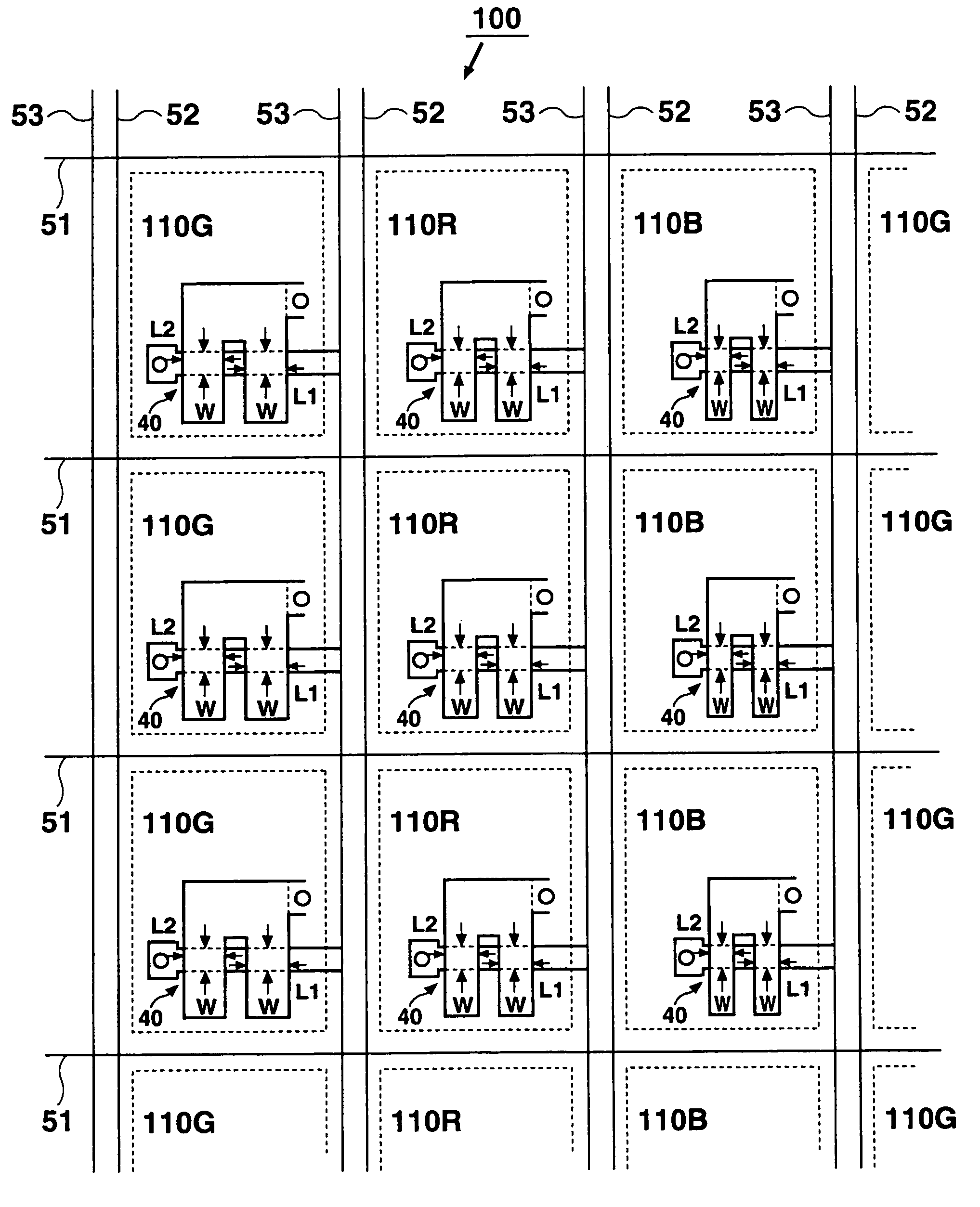
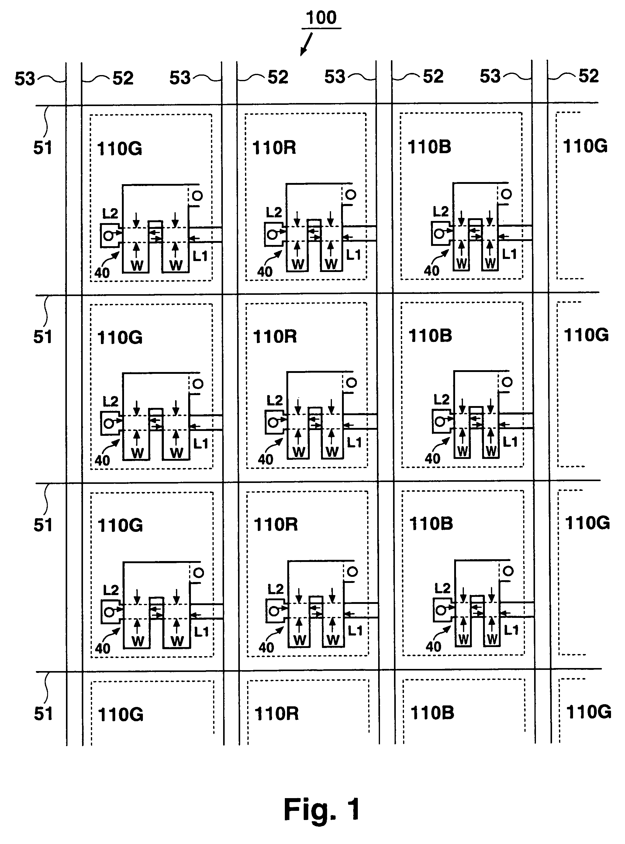
[0037]A display device according to the present invention is described next described.

[0038]FIG. 1 is a plan view of an EL display device 100. In FIG. 1, portions corresponding to an EL element driving TFT for supplying a current to an EL element are shown enlarged.

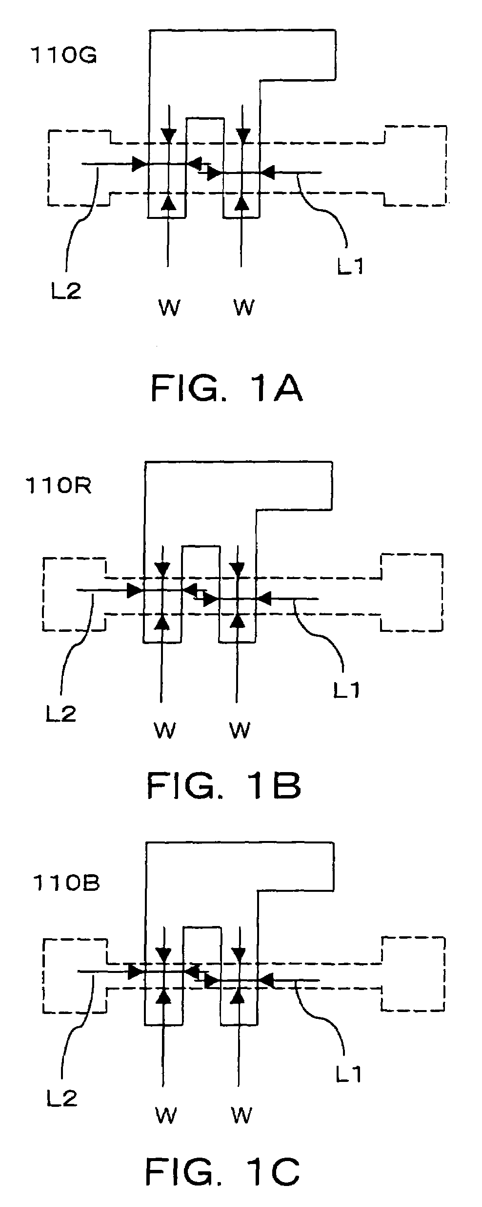
[0039]The figure illustrates an example in which the display pixels emit either red (110R), green (110G), or blue (110b). Among the components of a display pixel shown in the above-described FIG. 3, the only components shown enlarged in FIG. 1 are the gates 41 and the active layer 43 including the channel 43c, source 43s, and drain 43d of a driving TFT 40 arranged within a display pixel.

[0040]As can be seen in FIG. 1, in the EL display device 100, a plurality of gate signal lines 51 are arranged in a horizontal direction in the figure, and a plurality of power source lines 52 and drain signal lines 53 are arranged in a vertical direction in the figure. These lines 51 and 53, and 51 and 52, intersect one another.

[0041]As s...


PUM


Abstract

EL display elements are configured by sequentially laminating an anode, an emissive layer and a cathode, and emit light of R, G, and B. Each EL display element is supplied with a drive current from an EL element driving TFT. The transistor sizes of the EL element driving TFTs connected to the display pixels for respective colors are designated such that the size of the TFT for a green display pixel including an EL element having the highest emissive efficiency is the smallest, and the sizes of the TFTs for red and blue display pixels having sequentially decreasing emissive efficiency are made sequentially larger.

Description

BACKGROUND OF THE INVENTION[0001]1. Field of the Invention[0002]The present invention relates to a display device using a self-emissive element such as an electroluminescence (hereinafter referred to as “EL”) element and a thin film transistor (hereinafter referred to as “TFT”).[0003]2. Description of the Related Art[0004]In the recent years, display devices using EL elements, which are self-emissive elements, have gained attention as the display devices that may replace CRTs and LCDs.[0005]Research is being directed to development of display devices using TFTs as the switching elements for driving the EL elements.[0006]FIG. 2 is an equivalent circuit diagram of a conventional organic EL display device. FIG. 3 is a plan view of the organic EL display device showing an area around a display pixel. FIG. 4A is a cross-sectional view taken along line A—A of FIG. 3, while FIG. 4B shows a cross-sectional view taken along line B—B of FIG. 3. FIG. 5 illustrates the arrangement of display pi...

Claims


Application Information

Patent Timeline
Patent Type & Authority Patents(United States)
IPC IPC(8): G09G3/30G09F9/30H01L27/12H01L27/32H01L29/786H01L51/50H05B33/12H05B33/14H05B33/26H05B44/00
CPCH01L27/12H01L29/78645H01L27/3262H01L27/3211H10K59/35H10K59/1213
Inventor YAMADA, TSUTOMU
Owner SANYO ELECTRIC CO LTD
Why Eureka
Try Eureka