Memory devices, systems and methods using selective on-die termination

a memory device and on-die termination technology, applied in the field of memory systems, can solve the problems of difficult arrangement of a termination circuit on the system board, operation of the on-die-termination circuit, and undesirable amount of energy dissipation through the on-die-termination circui

Inactive Publication Date: 2006-08-15
SAMSUNG ELECTRONICS CO LTD
View PDF3 Cites 29 Cited by
  • Summary
  • Abstract
  • Description
  • Claims
  • Application Information

AI Technical Summary

Benefits of technology

[0007]In some embodiments of the present invention, a memory system includes first and second memory devices in respective independently selectable banks and having commonly connected data terminals and commonly connected memory control signal terminals, e.g., devices in respective first and second independently selectable memory banks that share common data lines and common memory control signal lines, such as column address strobe, row address strobe, write enable, and address signal lines. The first and second memory devices include respective selective on-die termination (ODT) circuits configured to selectively provide first and second termination impedances at their respective data terminals responsive to a memory control signal at the commonly connected memory control signal terminals. The selective ODT circuits may provide the first termination impedance responsive to a memory write operation, and may provide the second termination impedance responsive to a memory read operation and / or expiration of a predetermined time interval following termination of the memory write operation. Preferably, the first termination impedance is less than the second termination impedance, and the selective ODT circuits provide the first termination impedance responsive to the memory write operation irrespective of which of the first and second memory devices is being written to.
[0008]In further embodiments of the present invention, each of the ODT circuits includes an ODT control circuit configured to receive a memory control signal and operative to generate an ODT control signal responsive to the memory control signal. The ODT circuits also include a termination circuit configured to receive the ODT control signal and to selectively provide the first and second termination impedances at the data terminal of the memory device responsive to respective first and second states of the ODT control signal.
[0009]The ODT control circuit may comprise a command decoder operative to produce a write enable signal, a dummy write enable signal, a read signal and dummy read signal responsive to the memory control signal, a first OR gate configured to logically OR the write enable signal and the dummy write enable signal to produce an ODT enable signal, a second OR gate configured to logically OR the read signal and the dummy read signal to produce an ODT disable signal, and an ODT control signal generating circuit configured to receive the ODT enable signal and the ODT disable signal and to generate the ODT control signal therefrom. The termination circuit may include first and second resistors having first terminals connected to the data terminal and first and second transistors that couple and decouple second terminals of respective ones of the first and second transistors to and from respective ones of a power supply node and a signal ground node responsive to the ODT control signal.
[0010]In further embodiments of the invention, memory devices with selective ODT capability may be provided. Such a memory device may include a data terminal, a memory control signal terminal, and a selective ODT circuit configured to selectively provide first and second termination impedances at the data input terminal responsive to a memory control signal at the memory control signal terminal. In some method embodiments of the present invention, in a multi-bank memory system that includes first and second memory devices having commonly connected data terminals and commonly connected memory control signal terminals, first and second on-die termination (ODT) impedances are selectively provided at the data terminals responsive to a memory control signal at the commonly connected memory control signal terminals.

Problems solved by technology

However, as the number of signal lines arranged on the system board increases, it may become difficult to arrange a termination circuit on the system board.
Although this method may be simple, it has the potential problem that the on-die-termination circuit is operated even when unneeded, that is, when data are not input to the system.
Accordingly, an undesirable amount of energy may be dissipated through the on-die-termination circuit.
Accordingly, the more data input / output (or input) pads of the memory, the more on-die-termination circuits are needed, so the energy wasted by the on-die-termination circuits can become significantly large.

Method used


Image

  • Memory devices, systems and methods using selective on-die termination
  • Memory devices, systems and methods using selective on-die termination
  • Memory devices, systems and methods using selective on-die termination

Examples


Embodiment Construction

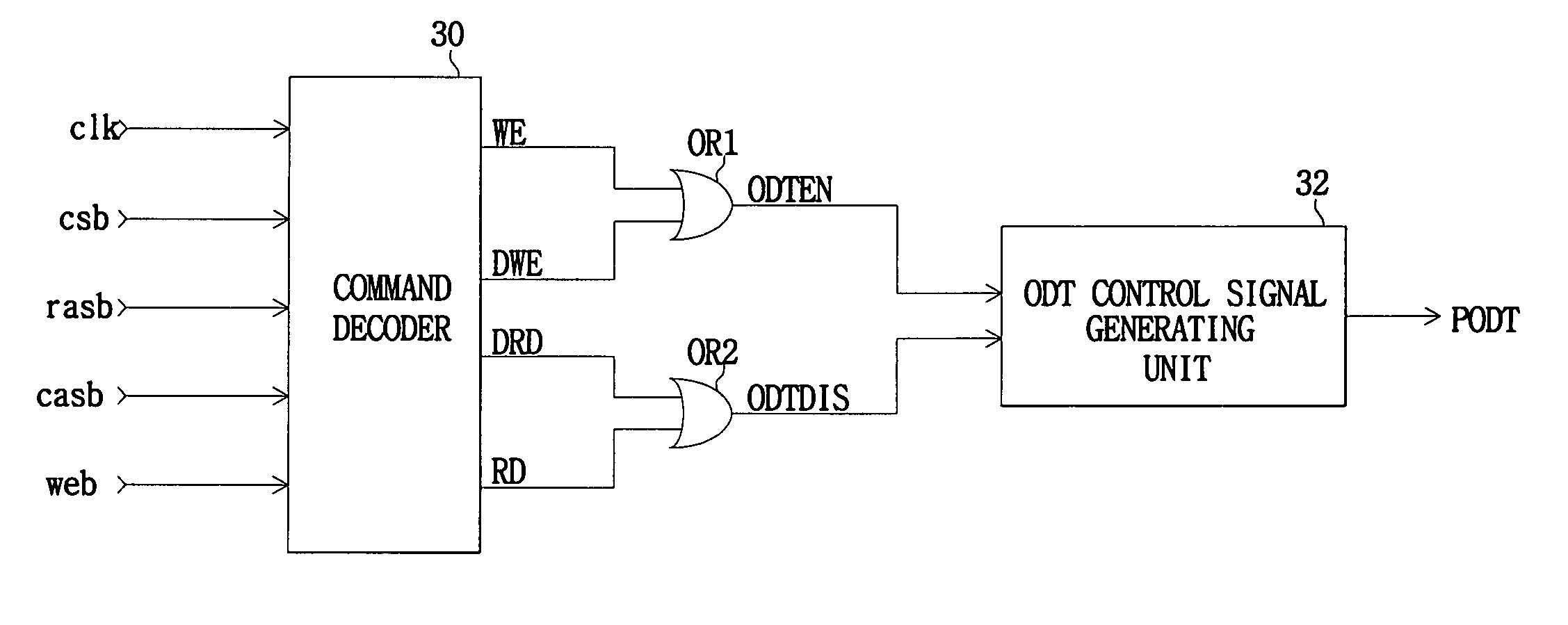
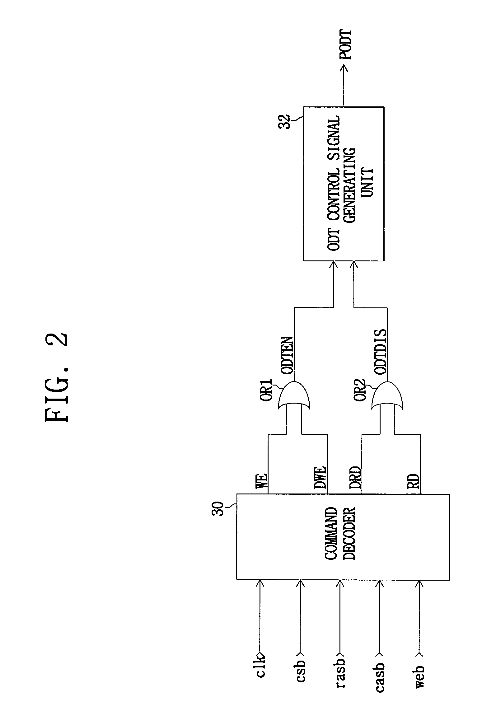
[0017]The present invention now will be described more fully with reference to the accompanying drawings, in which exemplary embodiments of the invention are shown. This invention may, however, be embodied in many different forms and should not be construed as being limited to the embodiments set forth herein; rather, these embodiments are provided so that this disclosure will be thorough and complete, and will fully convey the concept of the invention to those skilled in the art. In the drawings, when an element is referred to as being “connected” or “coupled” to another element, it can be directly connected or coupled to the other element or intervening elements may be present. In contrast, when an element is referred to as being “directly connected” or “directly coupled” to another element, there are no intervening elements present. Like reference numerals refer to like elements throughout.

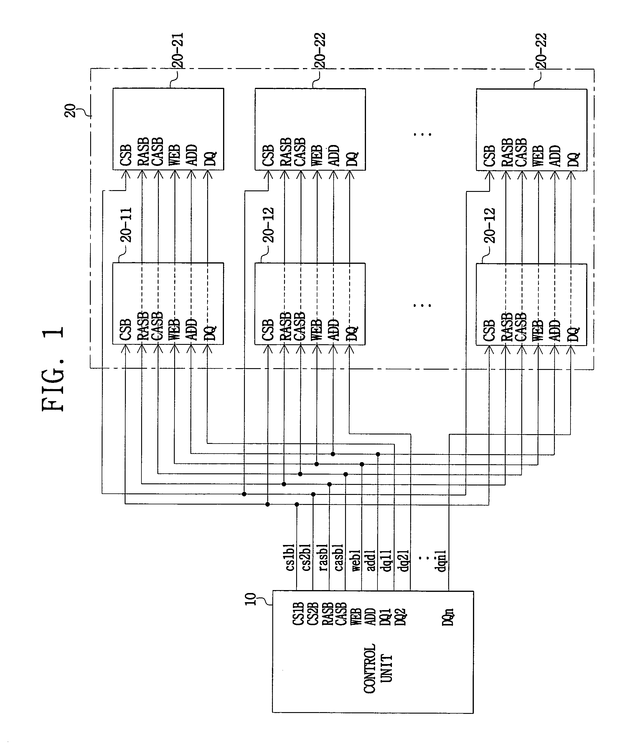
[0018]FIG. 1 is a schematic diagram illustrating a general dual bank memory system 100 acco...


PUM


Abstract

A memory system includes first and second memory devices having commonly connected data terminals and commonly connected memory control signal terminals, e.g., devices in respective first and second independently selectable memory banks that share common data lines and common memory control signal lines, such as column address strobe, row address strobe, write enable, and address signal lines. The first and second memory devices includes respective selective on-die termination (ODT) circuits configured to selectively provide first and second termination impedances at their respective data terminals responsive to a memory control signal at the commonly connected memory control signal terminals. The selective ODT circuits may produce the first termination impedance responsive to a memory write operation, and may produce the second termination impedance responsive to a memory read operation and/or expiration of a predetermined time interval following termination of the memory write operation. Preferably, the first termination impedance is less than the second termination impedance, and the selective ODT circuits provide the first termination impedance responsive to the memory write operation irrespective of which of the first and second memory devices is being written to.

Description

[0001]This U.S. nonprovisional patent application claims priority under 35 U.S.C. § 119 of Korean Patent Application 2003-30350 filed on May 13, 2003, the entire contents of which are hereby incorporated by reference.BACKGROUND OF THE INVENTION[0002]The present invention relates to memory systems, and more particularly, to signal termination in memory systems.[0003]One conventional signal termination technique terminates a signal by connecting a termination resistor and a termination voltage to signal lines arranged on a system board. However, as the number of signal lines arranged on the system board increases, it may become difficult to arrange a termination circuit on the system board.[0004]To solve the above problem, on-die-termination techniques have been developed. One conventional on-die-termination technique terminates a signal by arranging a termination circuit on an integrated circuit die, rather than on the system board. This can enhance arrangement of signal lines on the...

Claims


Application Information

Patent Timeline
Patent Type & Authority Patents(United States)
IPC IPC(8): G11C7/00G11C5/06G11C7/10
CPCG11C5/063G11C7/1048G11C7/10
Inventor KWAK, JIN-SEOKJANG, SEONG-JINJUN, YOUNG-HYUN
Owner SAMSUNG ELECTRONICS CO LTD
Why Eureka
Try Eureka