Lead frame, manufacturing method of the same, and semiconductor device using the same

a manufacturing method and lead frame technology, applied in semiconductor devices, semiconductor/solid-state device details, electrical apparatus, etc., can solve the problem that the arrangement pitch of the electrode cannot be fixed by flip-chip bonding

Inactive Publication Date: 2006-09-05
LAPIS SEMICON CO LTD
View PDF5 Cites 75 Cited by
  • Summary
  • Abstract
  • Description
  • Claims
  • Application Information

AI Technical Summary

Benefits of technology

[0012]The present invention has been made with the foregoing problems in mind. Accordingly, objects of the present invention are to provide a lead frame which enables mounting of a semiconductor element that is conventionally unmountable through flip chip bonding by reducing a pitch of inner lead portions of a lead frame, a manufacturing method of the lead frame, and a semiconductor device which uses the lead frame.

Problems solved by technology

Because of this difference in arrangement pitches, a semiconductor element which has bonding electrodes of an arrangement pitch of 180 μm or lower cannot be mounted by flip chip bonding.

Method used


Image

  • Lead frame, manufacturing method of the same, and semiconductor device using the same
  • Lead frame, manufacturing method of the same, and semiconductor device using the same
  • Lead frame, manufacturing method of the same, and semiconductor device using the same

Examples


first embodiment

[0065]A constitution of a semiconductor device which uses the foregoing lead frame will be described by referring to FIGS. 5A and 5B.

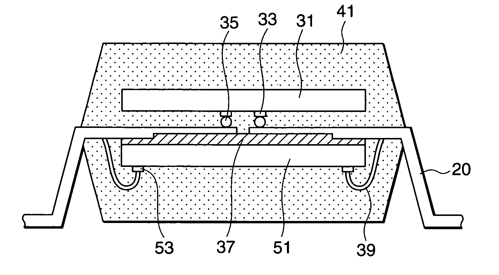
[0066]A first semiconductor element 31 is mounted on a lead frame 20. One surface of the first semiconductor element 31 is a circuit formation surface, and a bonding electrode 33 is disposed thereon as an electrode. A solder bump 35 is formed as a bump on the bonding electrode 33. By this solder bump 35, the bonding electrode 33 of the first semiconductor element 31 is connected through flip chip bonding to, especially, a tip 22a of a fine inner lead portion 22 of the lead frame 20.

[0067]A second semiconductor element 51 is stuck to a surface opposite a surface of the lead frame 20 on which the first semiconductor element 31 is mounted by a semiconductor element adhesive 37. This semiconductor element adhesive is an insulating adhesive which contains an epoxy resin.

[0068]A surface opposite a surface of the second semiconductor element 51 stuck to the l...

second embodiment

[0071]A constitution of a second embodiment of a semiconductor device of the present invention will be described by referring to FIG. 8. A difference from the first embodiment is that an insulating resin, e.g., an epoxy resin 43, fills a space between an inner lead portion 21 of a lead frame 20 and a first semiconductor element 31.

[0072]A reason for the disposition of the insulating resin layer of the epoxy resin 43 or the like is as follows. When a mold resin is disposed to envelope the semiconductor element, a bonding metal wire or the like mounted on the lead frame 20, the mold resin enters the space between the inner lead portion 21 of the lead frame 20 and the first semiconductor element 31. Application of pressure at the time of the resin entry may expand a gap between the first semiconductor element 31 and the inner lead portion 21. Consequently, there is a possibility of the generation of cracks in a solder bump.

[0073]However, according to the second embodiment, before moldi...

third embodiment

[0074]A constitution of a third embodiment of a semiconductor device of the present invention will be described by referring to FIG. 9.

[0075]According to the third embodiment, two first semiconductor elements 31a and 31b are mounted on a lead frame 20 in a state in which bonding electrodes face each other. One surface of each of the two first semiconductor elements 31a and 31b is a circuit formation surface, and a bonding electrode 33 is disposed thereon as an electrode. An Au bump 36 is formed as a bump on the bonding electrode 33. By the Au bump 36, the bonding electrode 33 is connected through an anisotropic conductive sheet 45 to front and back sides of a fine inner lead portion 22 of the lead frame 20. A tip 22a of the fine inner lead portion 22 of the lead frame 20 is etched to equal depths from both sides of a conductor plate to be removed, thereby being formed as a thin portion in a center of the conductor plate.

[0076]In this case, the anisotropic conductive sheet 45 has a s...


PUM


Abstract

In order to mount a semiconductor element of a small electrode pitch, an inner lead portion of a lead frame is made thin and narrow to reduce a pitch. Even a semiconductor element in which an electrode arrangement pitch is smaller than conventionally can be mounted by flip chip bonding, the number of components such as a wire is reduced, and a possibility of wire cutting or the like caused by vibration or the like during semiconductor device assembling is reduced. A fine inner lead formation scheduled area of a conductor plate is half-etched to make a plate thickness smaller than that in a peripheral area. Then, the fine inner lead formation scheduled area is patterned to form a fine inner lead portion 22. Especially, a width of a tip 22a of the fine inner lead portion 22 is set smaller than those of a middle inner lead portion 23 and an outer lead portion 25.

Description

BACKGROUND OF THE INVENTION[0001]1. Field of the Invention[0002]This invention relates to a lead frame, a manufacturing method of the lead frame, and a semiconductor device that is packaged by using the lead frame.[0003]2. Description of the Related Art[0004]The development of a technology of a semiconductor integrated circuit has heightened a request for high-density mounting especially by using multiple pins. In response to such a request, various packaging forms have been developed for semiconductor devices.[0005]There is a resin sealed package of a lead frame type as one of the packaging forms of the semiconductor devices. The resin sealed package has been widely used because of an inexpensive material and a shape that is suited to mass production.[0006]In the package of the lead frame type, a semiconductor element and an inner lead portion of the lead frame are generally connected to each other through a metal wire (e.g., see Patent Document 1 as identified below).[0007]A const...

Claims


Application Information

Patent Timeline
Patent Type & Authority Patents(United States)
IPC IPC(8): H01L23/495H01L23/50H01L21/56H01L21/60
CPCH01L23/49548H01L23/49575H01L21/563H01L24/83H01L2224/16H01L2224/48091H01L24/48H01L2224/83851H01L2924/01079H01L2924/1532H01L2924/07802H01L2224/2919H01L2224/48247H01L2924/00014H01L2924/3512H01L2924/00H01L2924/0665H01L2224/451H01L24/45H01L2924/14H01L2224/05573H01L2224/05568H01L2224/16245H01L2224/73265H01L2924/181H01L2224/32145H01L2924/00015H01L2224/05599H01L2924/00012
Inventor ICHIKAWA, SUNJI
Owner LAPIS SEMICON CO LTD
Why Eureka
Try Eureka