Capacitance detecting circuit and detecting method, and fingerprint sensor employing the same

a capacitance detection circuit and capacitance detection technology, applied in the direction of acquiring/reconfiguring fingerprints/palmprints, resistance/reactance/impedence, instruments, etc., can solve the problem of inability to obtain uniformly precise measurement, difficult to fully eliminate the effect of line layout or variation in stray resistance and stray capacitance of input selectors, and the resolution of detecting capacitance by the sensor elements is degraded. to achieve the effect o

Active Publication Date: 2006-09-05
SYNAPTICS INC
View PDF5 Cites 31 Cited by
  • Summary
  • Abstract
  • Description
  • Claims
  • Application Information

AI Technical Summary

Benefits of technology

[0013]The present invention has been made in view of the situation described above, and an object thereof is to provide a capacitance detecting circuit and detecting method and a fingerprint sensor employing the same with which the effect of external noise is suppressed to improve S / N ratio, allowing detection at a sufficient sensitivity of a small capacitance Cs and a capacitance change ACs of the capacitance Cs at an intersection (sensor element) of a column line and a row line.

Problems solved by technology

Thus, the mutual effect of the detecting lines is not fully eliminated, causing degradation in the resolution of detecting capacitance by the sensor elements.
Furthermore, in the conventional capacitance detecting circuit, although it is possible to decrease to a certain extent the effect of feed through of a sensor unit and switches respectively provided for the rows for introducing detection signals in a differential amplifier circuit, it is difficult to fully eliminate the effect of layout of lines or variation in stray resistance and stray capacitance of input selector.
Thus, the conventional capacitance detecting circuit has the drawback that it is not possible to obtain uniformly precise measurement results over the entire surface of a two-dimensional sensor such as an area sensor.

Method used


Image

  • Capacitance detecting circuit and detecting method, and fingerprint sensor employing the same
  • Capacitance detecting circuit and detecting method, and fingerprint sensor employing the same
  • Capacitance detecting circuit and detecting method, and fingerprint sensor employing the same

Examples


first embodiment

[0044

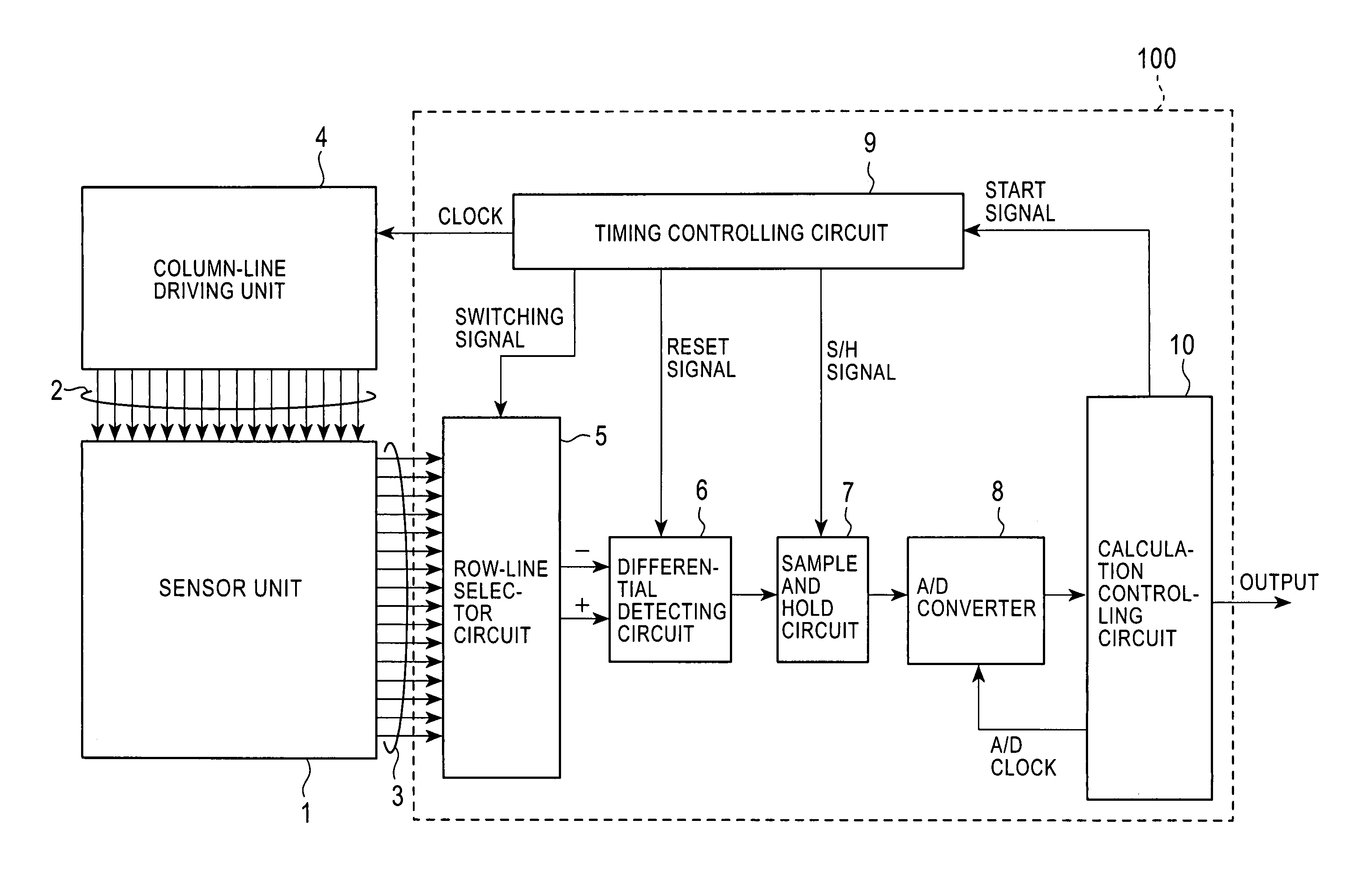
[0045]A capacitance detecting circuit according to a first embodiment of the present invention will be described with reference to FIG. 1. FIG. 1 is a block diagram showing an example configuration of a capacitance detecting circuit according to the first embodiment.

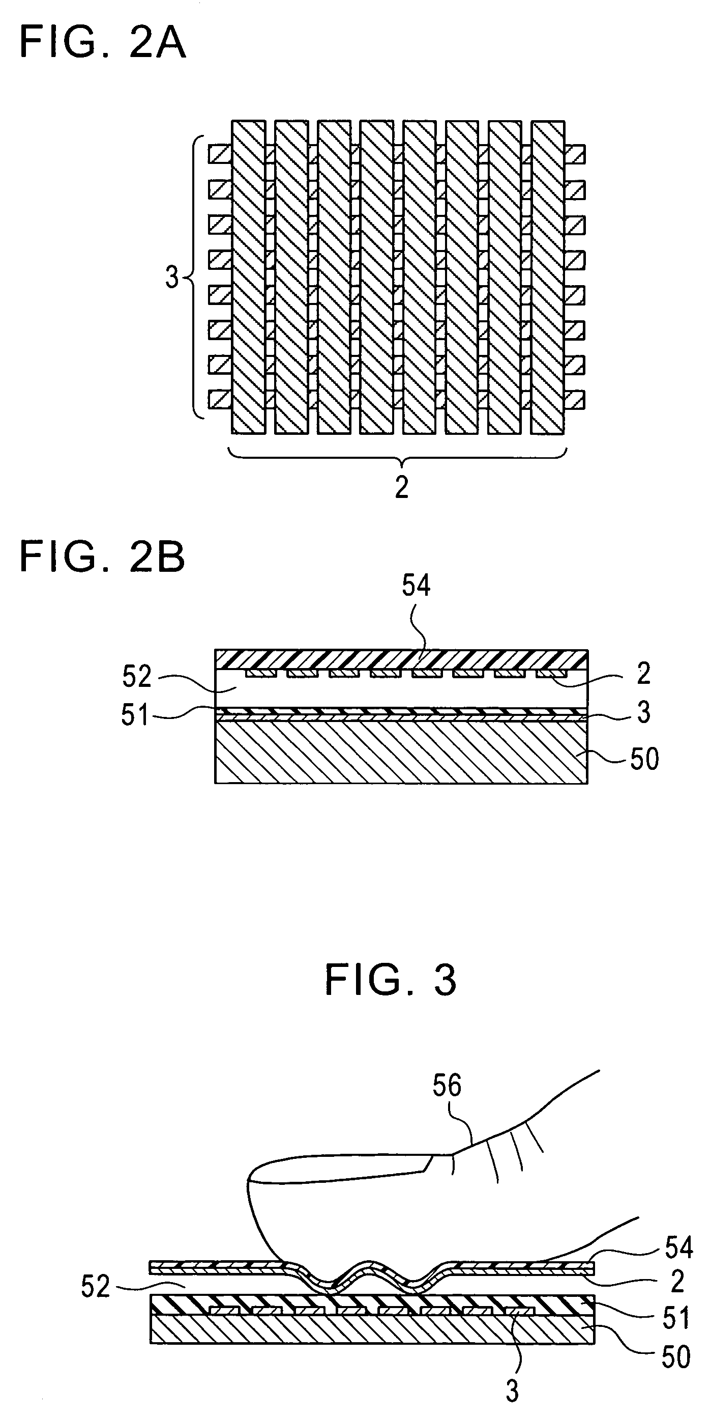
[0046]In a sensor unit 1, a plurality of column lines of a column-line set 2 and a plurality of row lines of a row-line set 3 cross each other in a matrix form, the respective intersections forming sensor elements (sensor elements 55 in FIG. 4).

[0047]FIG. 2A is a plan view of the sensor unit 1, and FIG. 2B is a sectional view thereof. As shown in FIG. 2A, the column lines of the column-line set 2 and the row lines of the row-line set 3, arranged at a pitch of, for example, 50 μm, cross each other. As shown in FIG. 2B, the row-line set 3 including the plurality of row lines is disposed on a substrate 50. Over a surface of the substrate 50, an insulating film 51 is laminated, a film 54 is provided over a surface of th...

second embodiment

[0133

[0134]Now, a capacitance detecting circuit according to a second embodiment of the present invention will be described with reference to FIG. 8. FIG. 8 is a block diagram showing an example configuration of the capacitance detecting circuit according to the second embodiment. In FIG. 8, parts corresponding to those of the capacitor detecting circuit 100 according to the first embodiment shown in FIG. 1 are designated by the same numerals, and descriptions thereof will be omitted. A capacitor detecting circuit 200 shown in FIG. 8 differs from the first embodiment shown in FIG. 1 in that the row-line selector 5 is divided into M row-line selectors 51 to 5M.

[0135]That is, the row lines R1 to Rn of the row-line set 3 are divided into M groups, and the row-line selectors 51 to 5M are respectively associated with row-line groups to be controlled, each consisting of n / M row lines.

[0136]Thus, the row-line selectors 51 to 5M are respectively associated with differential detecting circui...

third embodiment

[0144

[0145]A capacitance detecting circuit according to a third embodiment of the present invention will be described with reference to FIG. 9. FIG. 9 is a block diagram showing an example configuration of the capacitance detecting circuit according to the third embodiment. In FIG. 9, parts corresponding to those of the capacitance detecting circuit 100 according to the first embodiment shown in FIG. 1 will be designated by the same numerals, and descriptions thereof will be omitted. A capacitance detecting circuit 300 shown in FIG. 9 differs from the first embodiment shown in FIG. 1 in that as opposed to the first embodiment in which the reference capacitor R0 is provided to serve as a reference measurement voltage and is used as reference data for cumulative addition of measurement data, in the third embodiment, no special reference capacitor is provided, and row lines other than a subject row line for measurement in the row-line set 3 are connected to form a reference capacitor, ...


PUM


Abstract

A capacitance detecting circuit detects, in terms of voltage, change in capacitance at intersections of a plurality of column lines and a plurality of row lines crossing each other. The capacitance detecting circuit includes a column-line driving unit for driving a column line; a row-line selector for selecting a specific row line from the plurality of row lines; and a capacitance calculator for calculating a capacitance at an intersection of the specific row line and the driven column line based on a reference current that flows in relation to a reference capacitance and a current that flows in relation to the capacitance at the intersection.

Description

BACKGROUND OF THE INVENTION[0001]1. Field of the Invention[0002]The present invention relates to a capacitance detecting circuit and detecting method for detecting a small capacitance, and to a fingerprint sensor employing the same.[0003]2. Description of the Related Art[0004]Hitherto, as a fingerprint sensor, which is considered as most promising among techniques of biometrics, a pressure-sensitive capacitance sensor of a type in which column lines and row lines are formed at a predetermined pitch on surfaces of two films, respectively, the films being disposed opposing each other via an insulating film or the like with a predetermined gap provided therebetween, has been developed. In the pressure-sensitive capacitance sensor, when a finger is placed, the shapes of the films change according to the ridges and valleys of the fingerprint, and the gap between the column lines and the row lines change according to the change in the shapes of the films. Thus, the form of the fingerprint...

Claims


Application Information

Patent Timeline
Patent Type & Authority Patents(United States)
IPC IPC(8): G01R27/26G01B7/28G06K9/00
CPCG06K9/0002G06F3/044G06F3/0416G06F3/0446G06F3/04182G06V40/1306
Inventor UMEDA, YUICHIFUJIYOSHI, TATSUMIKAWAHATA, KEN
Owner SYNAPTICS INC
Why Eureka
Try Eureka