Touch-sensitive interface and method using orthogonal signaling

a touch-sensitive interface and orthogonal signaling technology, applied in the field of capacitance touch-screen sensing systems, can solve the problems of large amount of signal processing, difficult to accurately sense the very low level of capacitance change and the resulting signal change, etc., and achieve the effect of increasing the touch sensitivity

Inactive Publication Date: 2012-03-08
INTEL CORP
View PDF3 Cites 191 Cited by
  • Summary
  • Abstract
  • Description
  • Claims
  • Application Information

AI Technical Summary

Benefits of technology

[0020]It is an object of the invention to provide a capacitively coupled touch screen system having increased touch sensitivity without requiring increased supply voltage levels and without requiring use of a reduced “round robin” scanning rate.

Problems solved by technology

The coupling capacitances are very small, typically in the femto-farad range, and it is difficult to accurately sense the very low levels of capacitance change and resulting signal change on the various row conductors and column conductors.
However, a substantial challenge in obtaining an accurate computation of the touch point location is achieving sufficient signal power at the sense amplifier outputs 23-1,2 .
Another substantial challenge is achieving sufficiently fast scanning of the entire array to allow finger touch motion to be tracked and to allow new finger touch points to be accurately determined and rapidly displayed.
These challenges exist partly because the use of low-cost driver circuits limits the magnitude of the drive signals.
This is problematic because the amounts of capacitive coupling are so small that a large amount of signal processing is required to extract the desired signal out of all the noise and other incursions that are normally present.
The limited magnitude of the drive signals is also problematic because the touch screen must be scanned rapidly in order to track the position and / or movement of the user's finger tip (or tips) sufficiently rapidly to have the corresponding events displayed on a LCD display under layer 2 (FIG. 1) to appear to be instantaneously responsive to the user.
Accordingly, the duration of each of the previously mentioned sinusoidal bursts needs to be short, and the amount of required subsequent signal processing is large.
Unfortunately, the most readily available appropriate integrated circuit manufacturing processes may not permit the increased voltage needed for the driver circuits.
When higher signal voltage and signal power levels are required in touch screen integrated circuitry to achieve the desired touch screen performance, more costly, higher voltage integrated circuit fabrication processes are required.
It therefore becomes more difficult to integrate such circuitry with lower voltage, higher density, and lower cost circuitry that is ordinarily utilized for fabricating state-of-the-art integrated circuit touch screen control circuitry.

Method used


Image

  • Touch-sensitive interface and method using orthogonal signaling
  • Touch-sensitive interface and method using orthogonal signaling
  • Touch-sensitive interface and method using orthogonal signaling

Examples


Embodiment Construction

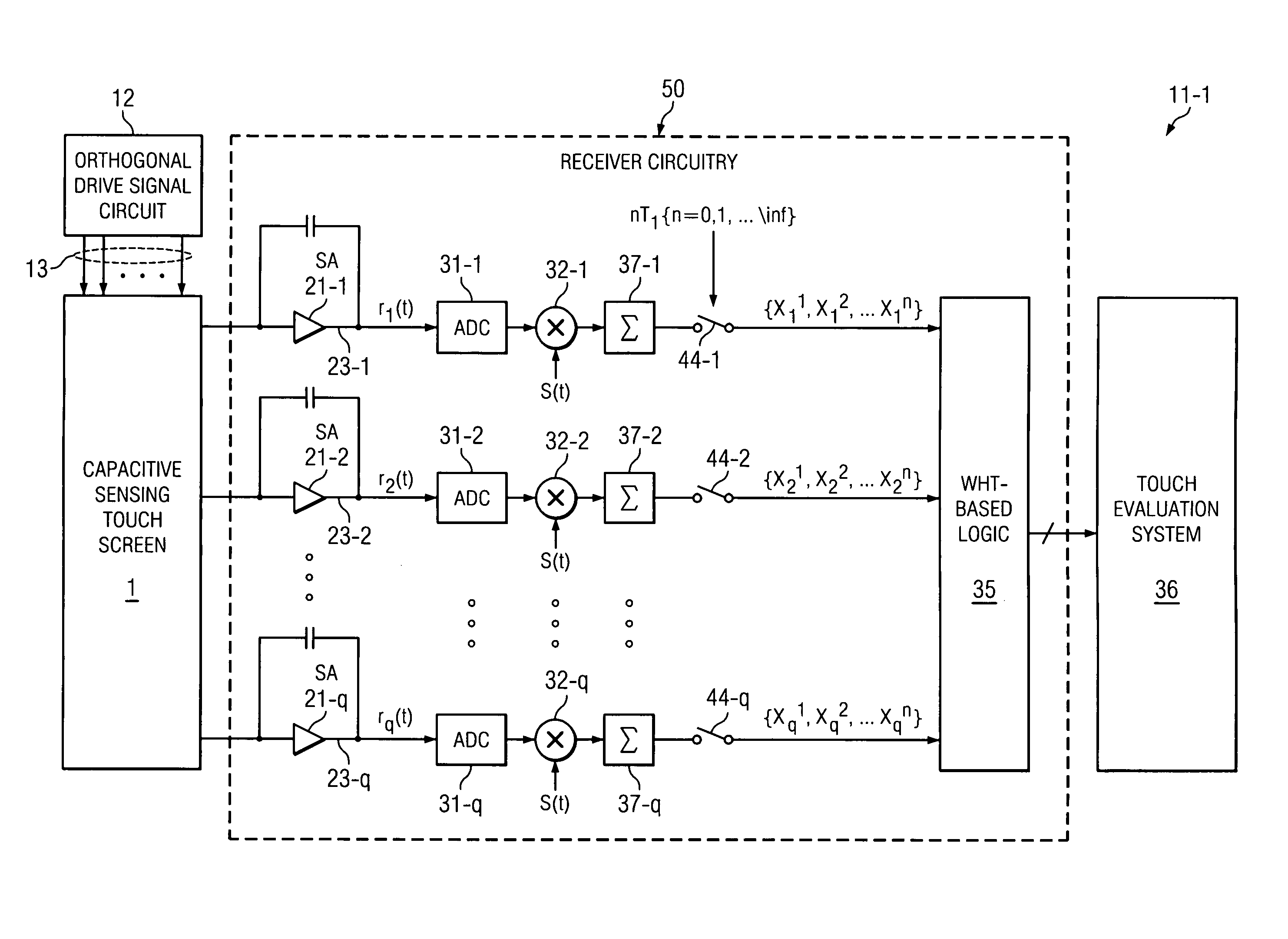
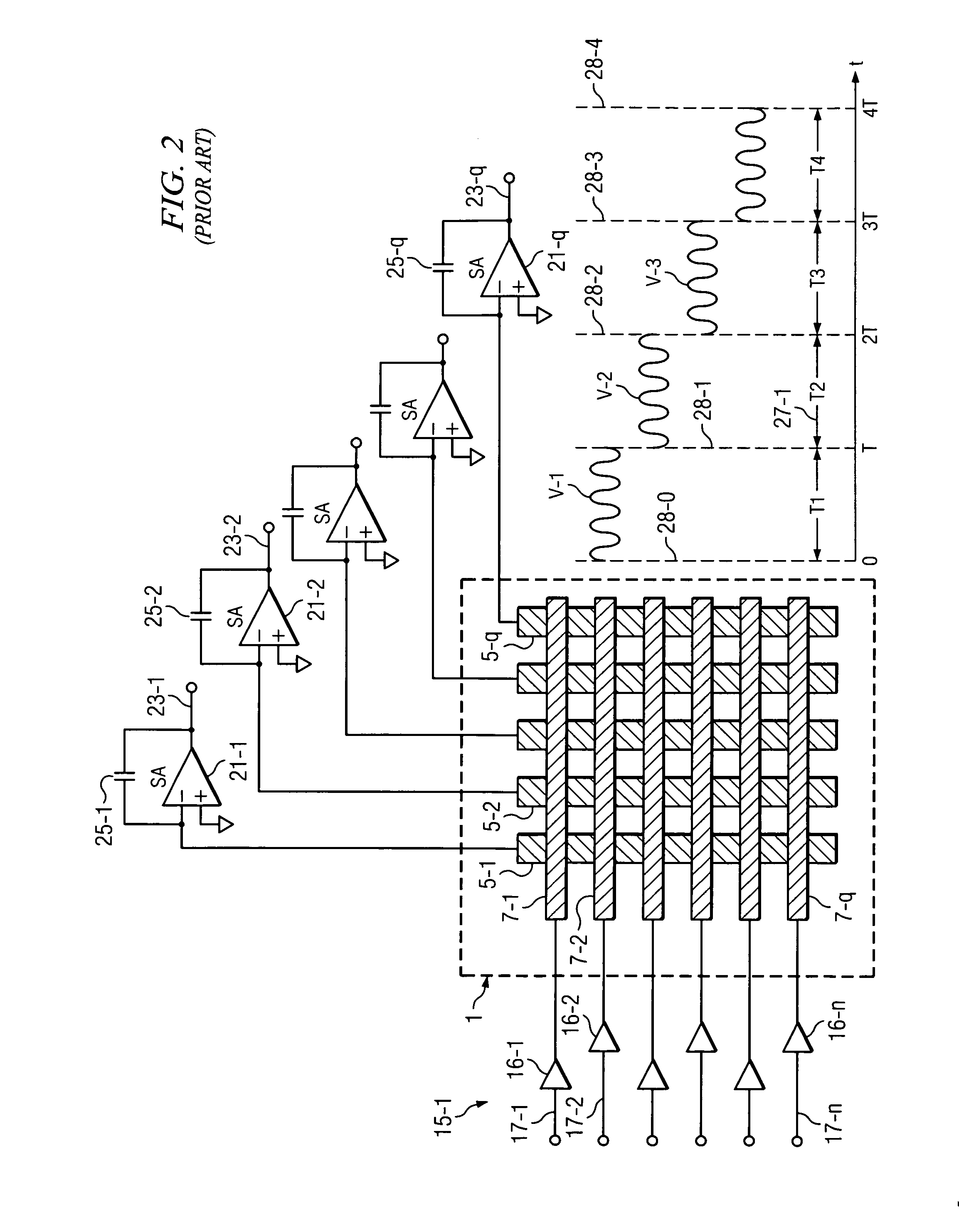
[0044]The present invention overcomes the above mentioned problems of the prior art by using orthogonal signals to excite a touch screen and to sense the resulting capacitively coupled signals generated on various grid conductors of the touch screen. All (or a substantial part) of the entire touch screen display can be excited simultaneously by the orthogonal excitation signals. The orthogonal excitation signals can be applied to touch screen grid conductors (such as row conductors 7-1,2 . . . n and column conductors 5-1,2 . . . q in FIG. 1) for much longer time intervals than would be possible using the previously mentioned round robin row and column scanning techniques. This allows signal energy levels to be increased without increasing supply voltage levels. Since a certain amount of signal energy is needed to overcome noise signals that may be present, such increased signal energy levels allow more accurate touch estimates to be achieved at lower signal power levels than is poss...


PUM


Abstract

A touch screen system includes a capacitive touch screen (1) including a plurality of row conductors (7-1,2 . . . n) and a column conductor (5-1). A plurality of cotemporaneous orthogonal excitation signals (S1(t), S2(t) . . . Sn(t)) are simultaneously driven onto the row conductors, respectively. The capacitively coupled signals on the column conductor may be influenced by a touch (10) on the capacitive touch screen. Receiver circuitry (50) includes a sense amplifier (21-1) coupled to generate an amplifier output signal (r1(t)) in response to signals capacitively coupled onto the column conductor. WHT-based circuitry (35) determines amounts of signal contribution capacitively coupled by each of the excitation signals, respectively, to the amplifier output signal.

Description

BACKGROUND OF THE INVENTION[0001]The present invention relates generally to capacitive touch screen sensing systems, and more particularly to providing capacitive touch screen scanning circuitry which generates substantially less noise than the prior art, provides faster scanning than the prior art, and can operate from lower supply voltage than the prior art.[0002]Touch sensing and multi-touch sensing displays are now widely used. There are a variety of approaches to touch sensing, and capacitive touch sensing is especially advantageous because it allows use of a hard touch surface (usually glass), and provides good performance.[0003]FIG. 1 shows a section view of a typical capacitive touch sensing screen 1, which includes a dielectric layer 2 that may be the top layer of a conventional LCD display. An optional conductive shield layer 3 may be provided on dielectric layer 2 to prevent signals in the LCD display from inducing electrical noise on column grid conductors and / or row gri...

Claims


Application Information

Patent Timeline
Patent Type & Authority Applications(United States)
IPC IPC(8): G06F3/044
CPCG06F3/044G06F3/0418G06F3/0446G06F3/04166G06F3/04182G06F3/04184
Inventor KRENIK, WILLIAM R.DABAK, ANAND
Owner INTEL CORP
Why Eureka
Try Eureka