Method for planning layout for LSI pattern, method for forming LSI pattern and method for generating mask data for LSI

a technology of lsi pattern and lsi pattern, which is applied in the direction of photomechanical treatment originals, instruments, and total factory control, etc., can solve the problem of increasing the difficulty of design rule concerning the extension size, the actual transfer pattern size is likely to deviate from the original design one, and the shrinkage rate becomes more and more difficult to achiev

Inactive Publication Date: 2006-09-05
PANASONIC CORP
View PDF12 Cites 219 Cited by
  • Summary
  • Abstract
  • Description
  • Claims
  • Application Information

AI Technical Summary

Benefits of technology

[0022]An object of the present invention is performing optical proximity corrections effectively in such a manner as to downsize an LSI just as intended and to form circuit patterns that will make the LSI fully operative.
[0025]According to the inventive method for planning an LSI pattern layout, optical proximity corrected patterns are generated first, and then a design rule defining circuit patterns is changed to make the corrections effective. Thus, the present invention eliminates a situation, where optical proximity corrections are no longer applicable to a mask pattern formed by transferring a designed pattern, as is often the case with the prior art.
[0027]In another embodiment of the present invention, the step of making the re-placement preferably includes the step of forming multiple re-placement patterns and selecting one of the re-placement patterns that minimizes a total circuit area.
[0043]According to the second inventive LSI mask data generating method, specifications of cell-level corrected patterns are set for the circuit patterns belonging to the first group of corrected patterns, and those circuit patterns are registered at a cell library. Thereafter, when mask data is generated, cell- and chip-level corrected patterns with a huge data volume are made using the cell library. Accordingly, that huge volume of data can be managed more easily.
[0051]According to the fifth inventive LSI mask data generating method, specifications of interlayer corrected patterns are set for the circuit patterns belonging to the first group of corrected patterns, and those circuit patterns are registered at a cell library. Thereafter, when mask data is generated, interlayer and intralayer corrected patterns with a huge data volume are made using the cell library. Accordingly, that huge volume of data can be managed more easily.

Problems solved by technology

That is to say, if the feature size of an originally designed pattern is automatically applied to the mask pattern, then the size of the actually transferred pattern is likely to deviate from the originally designed one.
This problem is particularly noticeable in a transistor, which plays a key role in determining the operability of an LSI.
These days, however, it has become more and more difficult to attain this shrinkage rate just by introducing a new system or improving the process.
Thus, it has become more and more difficult for the design rule concerning the extension size 101c to achieve the 70% shrinkage rate.
(1) A design rule defined without taking proximity effect corrections into account would result in an excessively increased mask size.
Accordingly, if the size deviation was simply expected and a design rule was defined based on the result without estimating how much the deviation can be reduced by forming an OPC pattern, then the mask size determined would be unnecessarily large.
Thus, the process conditions defined are not always best suited to the placement rule for the OPC patterns.
Actually, though, the process conditions are variable during the fabrication process, thus making the actual size non-uniform due to the variation.
(3) Although final process conditions for an LSI are determined just before the actual fabrication thereof, details of OPC patterns cannot be defined until specific process conditions are determined.
However, since the process conditions are determined just before the fabrication, details of OPC patterns cannot be defined at an early stage.
Accordingly, it is difficult to design circuit patterns for a cell library in view of final OPC patterns to solve the problem (1).
Accordingly, if a circuit is designed such that all the actual sizes thereof are reduced by 70% compared to the older generation, then unnecessarily stringent conditions will be imposed on the LSI fabrication, thus making it much harder to obtain a desired LSI.

Method used


Image

  • Method for planning layout for LSI pattern, method for forming LSI pattern and method for generating mask data for LSI
  • Method for planning layout for LSI pattern, method for forming LSI pattern and method for generating mask data for LSI
  • Method for planning layout for LSI pattern, method for forming LSI pattern and method for generating mask data for LSI

Examples


embodiment 1

[0081]Hereinafter, a first embodiment of the present invention will be described with reference to the accompanying drawings.

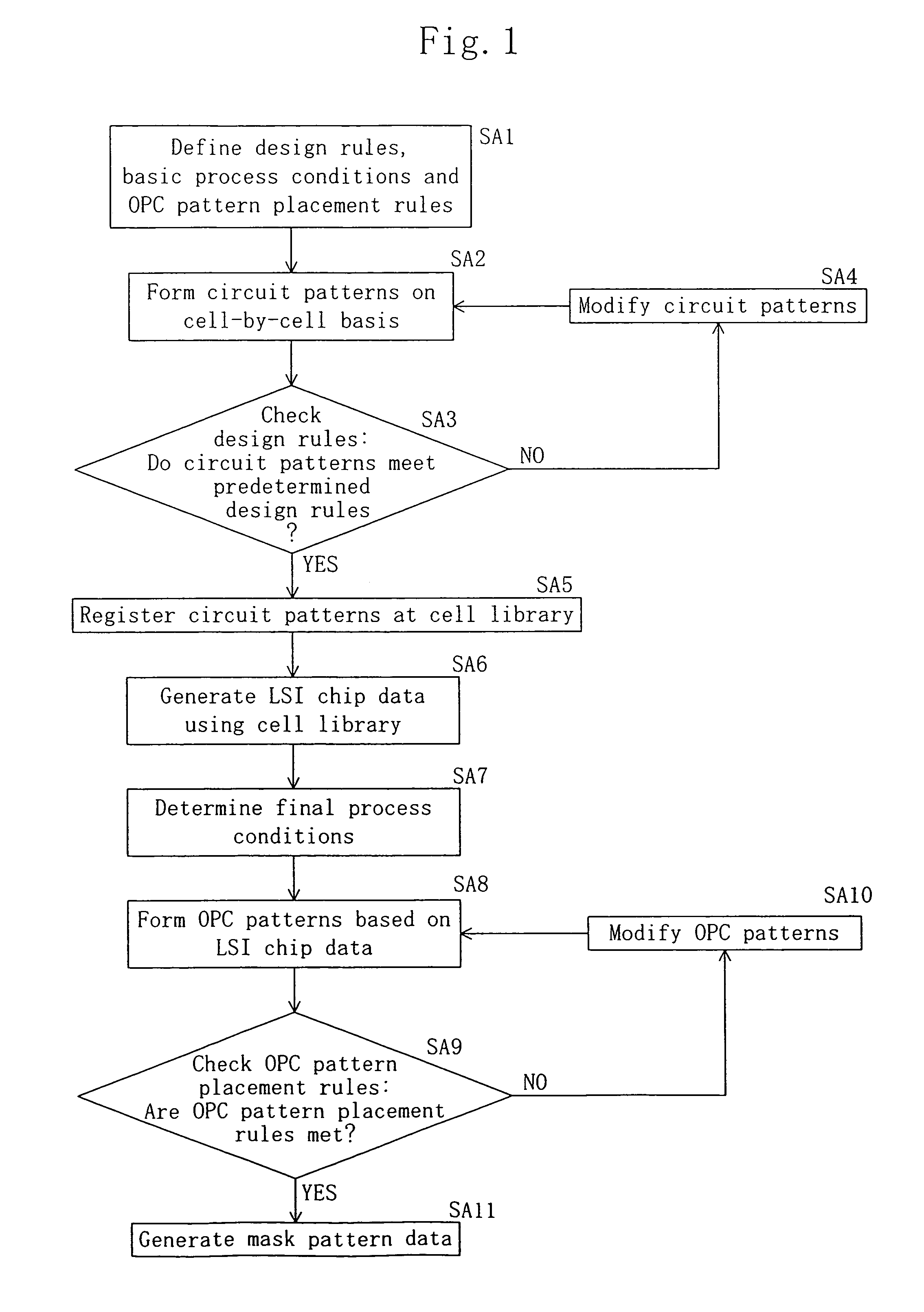
[0082]According to the first embodiment, a design rule is determined so as to satisfy the conditions that should be met to form OPC patterns of the type making optical proximity corrections effective when an LSI is fabricated. And circuit patterns are designed and mask pattern data is generated in accordance with the design rule determined.

[0083]Also, the OPC patterns are made from the circuit patterns in accordance with the design rule that makes the OPC effective, and basic process conditions are optimized based on the OPC patterns obtained. In this specification, the OPC can be regarded as “effective” when a pattern, which has been actually transferred onto a region with substantially the same area as an originally designed circuit pattern using this OPC pattern, ensures proper operation for a resulting circuit.

[0084]FIG. 1 illustrates a processing flow of ...

embodiment 2

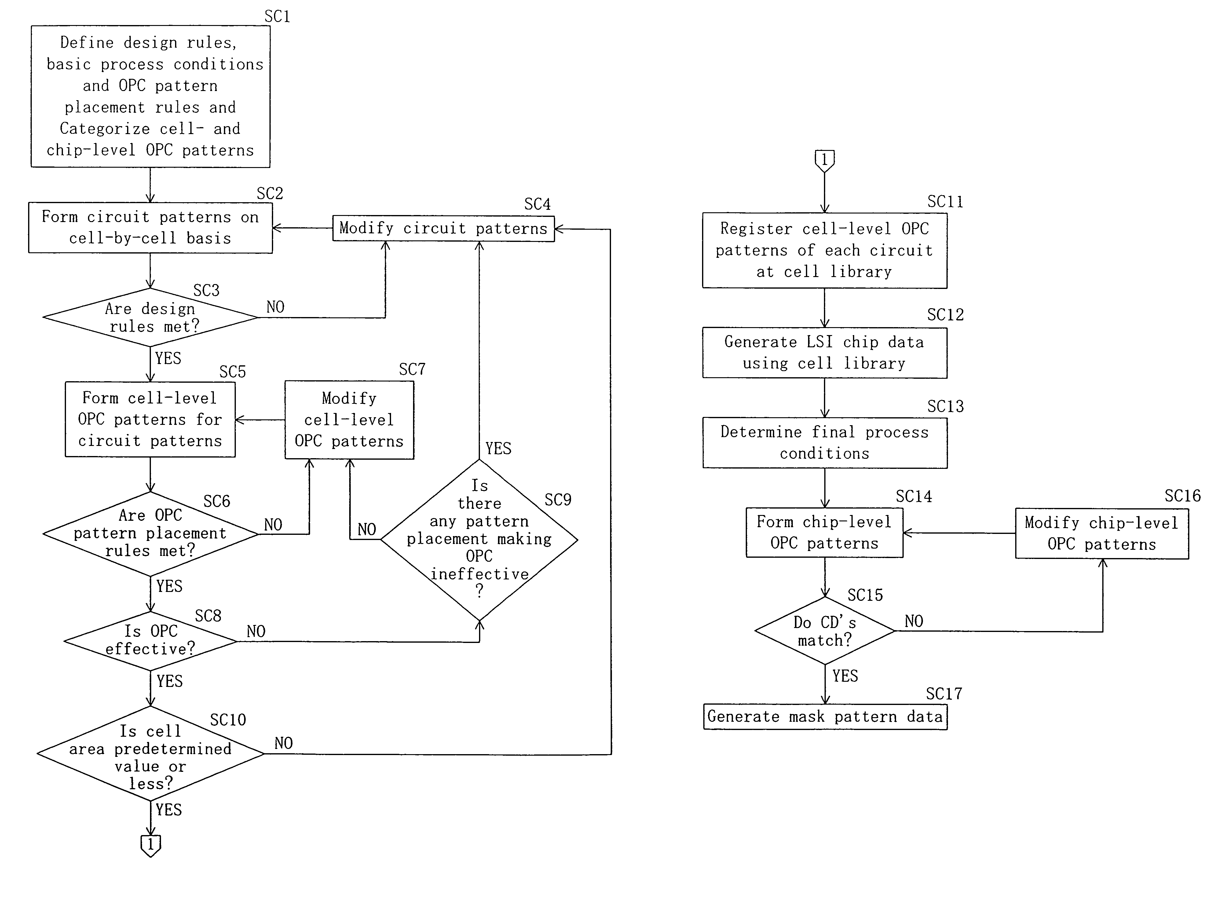
[0122]Hereinafter, a second embodiment of the present invention will be described with reference to the accompanying drawings. According to the second embodiment, design rules are determined so as to satisfy the conditions that should be met to form required OPC patterns as in the first embodiment.

[0123]And circuit patterns are designed and mask pattern data is generated in accordance with the design rules determined. In particular, according to the second embodiment, each cell (basic circuit) being designed can be individually checked for the effectiveness of the OPC. Thus, a cell area can be reduced on a cell-by-cell basis.

[0124]FIGS. 10 and 11 illustrate a processing flow of an LSI mask data generating method according to the second embodiment.

[0125]First, in Step SC1 shown in FIG. 10, design rules, basic process conditions and OPC pattern placement rules are determined. In this case, the design rules and the basic process conditions are determined as in Step SA1 shown in FIG. 1....

modified example of embodiment 2

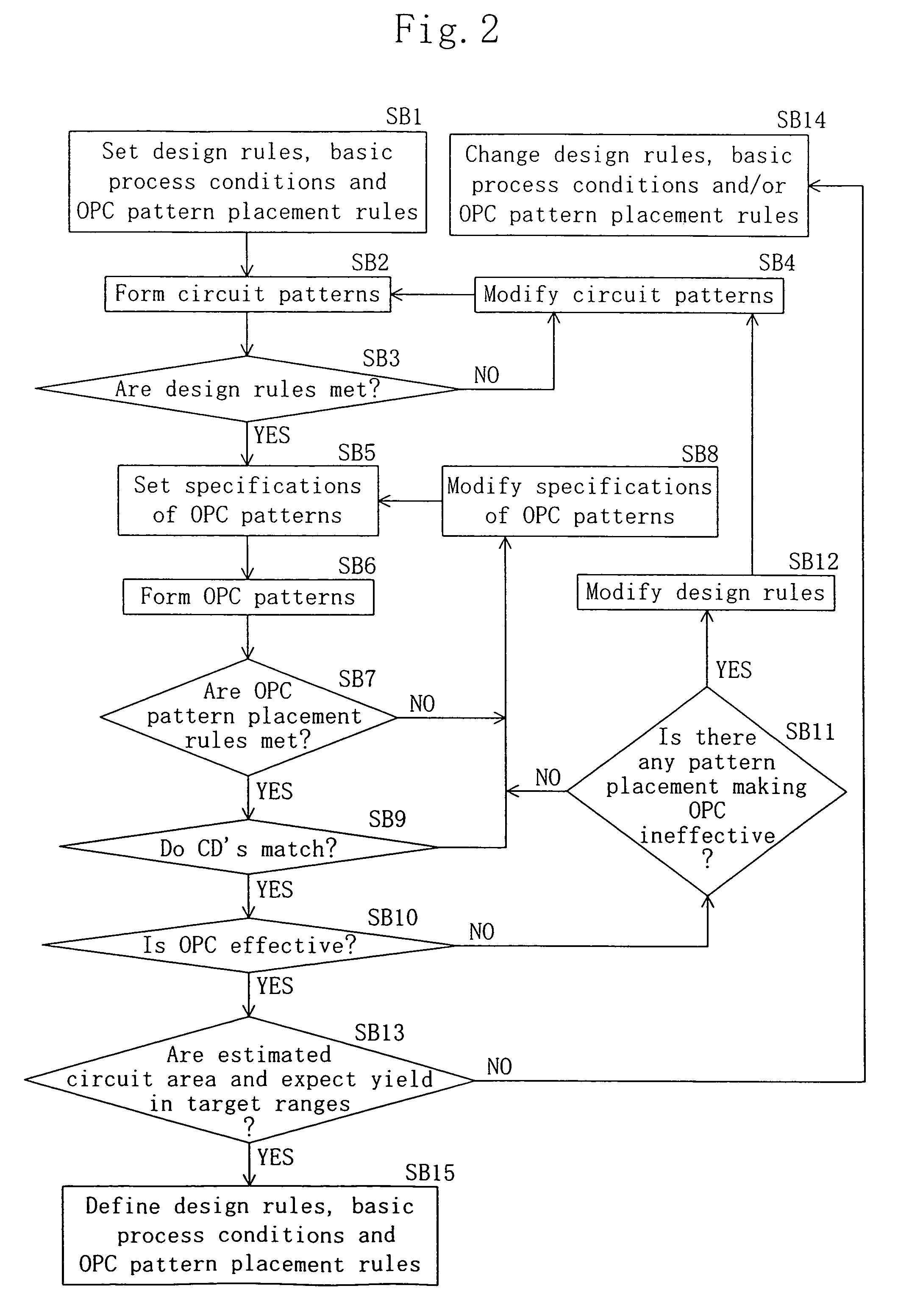
[0143]Hereinafter, a modified example of the second embodiment will be described with reference to the accompanying drawings.

[0144]FIGS. 13 and 14 illustrate a processing flow of an LSI mask data generating method according to a modified example of the second embodiment. In the second embodiment, cell-level OPC patterns are directly registered at the cell library in Step SC11. In contrast, according to this modified example, the step of making a cell-level OPC pattern includes the sub-steps of: setting the specification of the cell-level OPC pattern to be made; and making the cell-level OPC pattern to the specifications by a rules-based technique. In this manner, a circuit pattern and the specification of a cell-level OPC pattern associated with the circuit pattern can be registered at the cell library, instead of directly registering the cell-level OPC pattern.

[0145]The process steps SD1 through SD10 according to this modified example shown in FIG. 13 are different from the process...


PUM


Abstract

First, multiple circuit patterns, which will eventually make an LSI, are designed on a cell-by-cell basis, and an initial placement is made for the circuit patterns designed. Next, optical proximity corrections are performed on at least two of the circuit patterns that have been initially placed to be adjacent to or cross each other, thereby forming optical proximity corrected patterns out of the adjacent or crossing circuit patterns. Then, it is determined whether or not optical proximity corrections can be performed effectively using the corrected patterns. If the effectiveness of the corrections is negated, a design rule defining the circuit patterns is changed to make the corrections effective. Thereafter, the initially placed circuit patterns are placed again in accordance with the design rule changed.

Description

[0001]This application is a division of application Ser. No. 09 / 517,617 filed Mar. 3, 2000 which is now U.S. Pat. No. 6,691,297.BACKGROUND OF THE INVENTION[0002]The present invention relates to a method for planning a layout for an LSI pattern with optical proximity corrections ensured, a method for generating mask data and a method for forming an LSI pattern using these methods.[0003]Recently, as a semiconductor large-scale integrated circuit (LSI) device has been downsized, a photolithographic step, which is one of the main process steps of an LSI fabrication process, has been affected by optical proximity effects more and more seriously. Specifically, a deviation of a feature size of a pattern actually transferred onto a resist from that of a mask pattern formed on a reticle has almost reached a non-negligible level. That is to say, if the feature size of an originally designed pattern is automatically applied to the mask pattern, then the size of the actually transferred pattern...

Claims


Application Information

Patent Timeline
Patent Type & Authority Patents(United States)
IPC IPC(8): G06F17/50
CPCG06F17/5068G06F17/5081G06F17/5072G03F1/36G06F2217/12G03F1/68G06F30/392G06F2119/18G06F30/398G06F30/39Y02P90/02
Inventor MISAKA, AKIOODANAKA, SHINJI
Owner PANASONIC CORP
Why Eureka
Try Eureka