Liquid crystal display device and method of fabricating the same

a technology of liquid crystal display and liquid crystal, which is applied in the direction of instruments, non-linear optics, optics, etc., can solve the problems of color shifting, narrow viewing angle, and conventional lcd devices having longitudinal electric fields, so as to prevent color sifting and increase the viewing angle

Inactive Publication Date: 2006-09-19
LG DISPLAY CO LTD
View PDF15 Cites 5 Cited by
  • Summary
  • Abstract
  • Description
  • Claims
  • Application Information

AI Technical Summary

Benefits of technology

[0024]An advantage of the present invention is to provide a liquid crystal display device and a method of fabricating the same, which increase a viewing angle and prevent a color sift.
[0025]Another advantage of the present invention is to provide a liquid crystal display device and a method of fabricating the same, which provide uniform directions of liquid crystal molecules in all directions.

Problems solved by technology

However, the conventional LCD devices having the longitudinal electric field have a drawback in that they have a very narrow viewing angle.
However, the IPS-LCD device having the above-mentioned multidomains has a problem of color shifting depending on the viewing angles, because the liquid crystal molecules have long and thin shapes.

Method used


Image

  • Liquid crystal display device and method of fabricating the same
  • Liquid crystal display device and method of fabricating the same
  • Liquid crystal display device and method of fabricating the same

Examples


first embodiment

[0044]FIGS. 5A and 5B are plan views illustrating a liquid crystal display device according to a first exemplary embodiment of the present invention. FIG. 5A shows an array substrate including a thin film transistor and FIG. 5B shows a color first substrate facing the array substrate. In the present invention, common and pixel electrodes have a circular band or circular band shape.

[0045]As shown in FIG. 5A, on a first substrate 110, a gate line 112 is formed in a first direction and a data line 128 is formed in a second direction crossing the first direction. A common line 114 is formed in the first direction to be spaced apart from the gate line 112. It is understood that line refers to a structure that carries signal. It does not refer to or limit the shape of that structure. A thin film transistor (TFT) T is disposed at a crossing of the gate and data lines 112 and 128. The gate and data lines 112 and 128 define a pixel region P.

[0046]In the pixel region P, a pixel electrode 138 ...

second embodiment

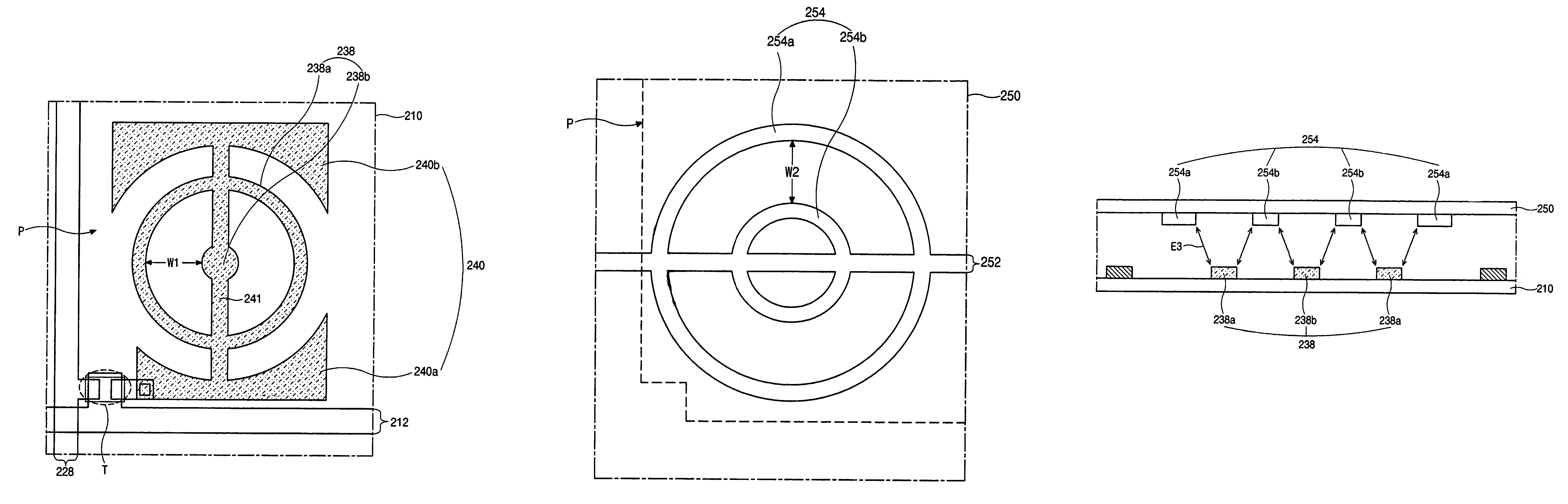
[0058]FIGS. 7A and 7B are plan views illustrating a liquid crystal display device according to the present invention. FIG. 7A shows an array substrate including a thin film transistor and FIG. 7B shows a color first substrate facing the array substrate.

[0059]In FIG. 7A, a common line and a common electrode may be omitted as compared with FIG. 5A, and other elements may have the same structures as elements of FIG. 5A.

[0060]As shown in FIG. 7A, on a first substrate 210, a gate line 212 and a data line 228 cross each other to define a pixel region P. A thin film transistor (TFT) T is disposed at a crossing of the gate and data lines 212 and 228.

[0061]A pixel electrode 238 is formed in the pixel region P. The pixel electrode 238 includes a first pixel electrode pattern 238a having a circular band shape and a second pixel electrode pattern 238b having a circular shape. The second pixel electrode pattern 238b is disposed inside the first pixel electrode pattern 238a.

[0062]A capacitor ele...

third embodiment

[0073]In FIG. 9, adjacent data lines 328 are formed on a first substrate 310, and a pixel region P is defined between the adjacent data lines 328. A pixel electrode 338, which includes first and second pixel electrode patterns 338a and 338b, is formed in the pixel region P on the first substrate 310. A common electrode 354, which includes first and second common electrode patterns 354a and 354b, is formed on a second substrate 350, which is disposed over and faces the first substrate 310. In the third embodiment, since the common electrode 354 and the data line 328 are formed on different substrates and electric interference between the common electrode 354 and the data line 328 is minimized, the common electrode 354 can be formed to correspond to the data line 328, and thus an aperture area may be widened.

[0074]Accordingly, in FIG. 9, the first common electrode pattern 354a is formed to overlap the data line 328, and a distance between the common electrode 354 and the pixel electro...


PUM

PropertyMeasurementUnit
angleaaaaaaaaaa
viewing anglesaaaaaaaaaa

Abstract

A liquid crystal display device includes gate and data lines on a first substrate and crossing each other to define a pixel region, a thin film transistor at a crossing of the gate and data lines, a pixel electrode connected to the thin film transistor and having a circular band shape, a common line on a second substrate spaced apart from and facing the first substrate, and a common electrode extending from the common line and having a circular band shape.

Description

[0001]This application claims the benefit of Korean Patent Application No. 2003-0092133, filed on Dec. 16, 2003, which is hereby incorporated by reference as if fully set forth herein.BACKGROUND OF THE INVENTION[0002]1. Field of the Invention[0003]The present invention relates to a liquid crystal display device and a method of fabricating the same.[0004]2. Discussion of the Related Art[0005]A liquid crystal display device uses the optical anisotropy and polarization properties of liquid crystal molecules to produce an image. Liquid crystal molecules have a definite orientational alignment based their long, thin shapes. That alignment direction can be controlled by an applied electric field. In other words, as an applied electric field changes, so does the alignment of the liquid crystal molecules. Due to the optical anisotropy, the refraction of incident light depends on the alignment direction of the liquid crystal molecules. Thus, by properly controlling an applied electric field,...

Claims


Application Information

Patent Timeline
Patent Type & Authority Patents(United States)
IPC IPC(8): G02F1/1343G02F1/1333G02F1/1362
CPCG02F1/134336G02F1/134363G02F1/133707G02F2201/121G02F2001/134318G02F2001/134381G02F1/136213G02F1/134318G02F1/134381G02F1/1343
Inventor LEE, YUN BOK
Owner LG DISPLAY CO LTD
Why Eureka
Try Eureka