
Method and apparatus for static phase offset correction

a static phase offset and correction method technology, applied in the field of microprocessors, to achieve the effect of reducing or eliminating the effect of static phase offset and best margin for both setups

Active Publication Date: 2006-09-19
ORACLE INT CORP
View PDF10 Cites 10 Cited by
  • Summary
  • Abstract
  • Description
  • Claims
  • Application Information

AI Technical Summary

Benefits of technology

[0014]In order to reduce or eliminate the effect of static phase offset (from the CPU clock signal) in the generation of the JBUS clock signal and achieve the best margin for both setup and hold times, embodiments in accordance with present invention generate a JBUS clock signal utilizing a CPU clock signal and a feedback signal of a phase lock loop (PLL) circuit used in generating the CPU clock signal from a system clock signal. The feedback signal of the PLL circuit has the same frequency as the system clock signal, and the same static phase offset as the CPU clock signal.

Problems solved by technology

Consequently, an alignment detection circuit used in generating the JBUS clock signal does not detect an alignment disparity between the feedback signal of the PLL circuit and the CPU clock signal due to static phase offset.

Method used


Image

  • Method and apparatus for static phase offset correction
  • Method and apparatus for static phase offset correction
  • Method and apparatus for static phase offset correction

Examples


Embodiment Construction

[0030]The invention will now be described in reference to the accompanying drawings. The same reference numbers can be used throughout the drawings and the following description to refer to the same or like parts.

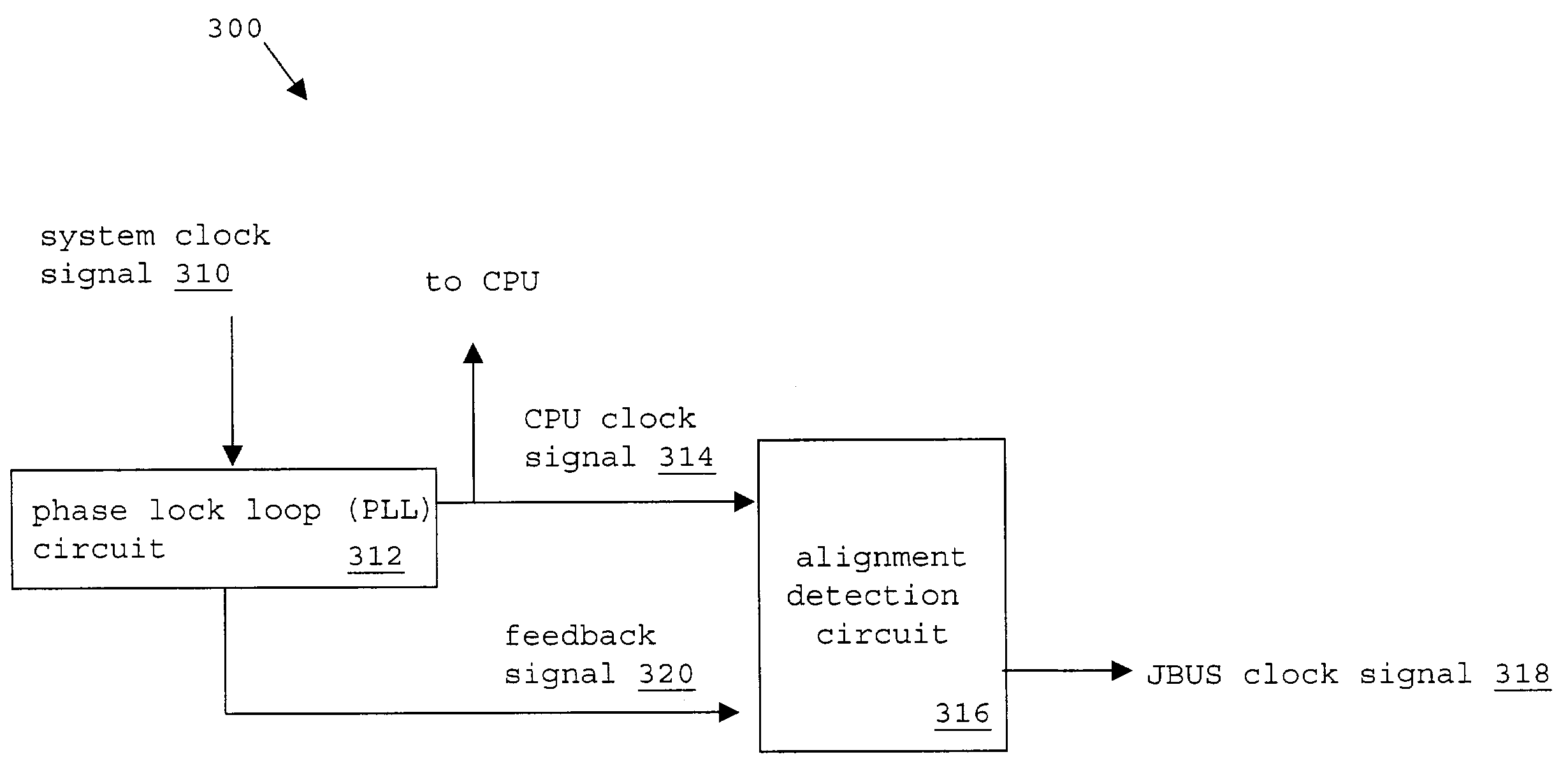
[0031]FIG. 3 illustrates a functional diagram of a static phase offset corrected clock alignment circuit 300 for generating a JBUS clock signal 318 utilizing a CPU clock signal 314 and a feedback signal 320 from a PLL circuit 312 in accordance with one embodiment of the present invention. In one embodiment of the invention shown in FIG. 3, a system clock signal 310 is input to phase lock loop (PLL) circuit 312 to generate CPU clock signal 314. PLL circuit 312 utilizes feedback signal 320 to maintain synchronization of CPU clock signal 314 with system clock signal 310. PLL circuits and the use of feedback signals in PLL circuits is well known to those of skill in the art and are, therefore, not further described herein to avoid detracting from the present invention.

[0032]In ...


PUM


Abstract

A CPU clock signal generated from a phase lock loop (PLL) circuit and a feedback signal of the PLL circuit are used in generating a JBUS clock signal. The CPU clock signal and the feedback signal include the same amount of static phase offset introduced by the PLL circuit. The CPU clock signal and the feedback signal are input to an alignment detection circuit and used in generating the JBUS clock signal. In one embodiment, the JBUS clock signal is generated in synchronization with the CPU clock signal and having the frequency of the feedback signal. The present invention reduces or eliminates misalignment of the leading edge of the JBUS signal with reference to a specific leading edge of the CPU clock signal due to the presence of static phase offset introduced by the PLL circuit.

Description

BACKGROUND OF THE INVENTION[0001]1. Field of the Invention[0002]The present invention is directed to the field of microprocessors, and more particularly, to alignment of clock signals in microprocessors.[0003]2. Description of Related Art[0004]Conventionally, many of the digital circuits that make up a microprocessor are synchronously designed to transfer a digital signal in accordance with a clock signal and, thus, require precise timing to function properly. To manage the timing requirements throughout the microprocessor, the microprocessor is typically divided up into several clock domains.[0005]When a digital signal travels across two clock domains, the clock signals used within the two clock domains should be synchronized so that the data signal will be received in a specific window of time in order for it to be utilized by a receiving component. Typically, this specific window of time is defined in terms of set up and hold times which define a period of time during which a dat...

Claims


Application Information

Patent Timeline
Patent Type & Authority Patents(United States)
IPC IPC(8): G06F1/12G06F1/10
CPCG06F1/10
Inventor HAN, ZHIGANGKHIEU, CONGNAGARAKANTI, KAILASHNATH
Owner ORACLE INT CORP
Learn More