Inspection system, inspection method, and method for manufacturing semiconductor device

a technology for semiconductor devices and inspection methods, applied in semiconductor/solid-state device testing/measurement, individual semiconductor device testing, instruments, etc., can solve the problems of shortening the turnaround time and difficulty in shortening the electric inspection process, so as to reduce the number of measuring potentials, improve the throughput of the inspection process, and facilitate the effect of attenuation

Inactive Publication Date: 2006-09-26
SEMICON ENERGY LAB CO LTD
View PDF10 Cites 191 Cited by
  • Summary
  • Abstract
  • Description
  • Claims
  • Application Information

AI Technical Summary

Benefits of technology

[0019]According to the above described structures of the present invention, a signal or power supply voltage can be supplied to an ID chip without contact. Further, as the number of ID chips becomes larger, the number of measuring a potential can be reduced drastically as that of a conventional one, and throughput of an inspection process can be improved.
[0020]In the case of an ID chip formed by using a semiconductor substrate, radio waves are blocked and a signal is easily attenuated since the semiconductor substrate serves as a conductor, thus it is difficult to send radio waves uniformly to all antennas of the ID chips. However, in the case of an ID chip formed by an insulating substrate such as a glass substrate or a plastic substrate, which is more difficult to prevent radio waves than a semiconductor substrate, radio waves can be sent more uniformly to all antennas of the ID chip as compared with the case of the ID chip using a semiconductor substrate.

Problems solved by technology

Therefore, it is difficult to shorten the time of an electric inspection process even if an inspection system (apparatus) having the anti-collision function is used, which leads to prevent TAT (Turnaround time) from being shortened.

Method used


Image

  • Inspection system, inspection method, and method for manufacturing semiconductor device
  • Inspection system, inspection method, and method for manufacturing semiconductor device
  • Inspection system, inspection method, and method for manufacturing semiconductor device

Examples


embodiment 1

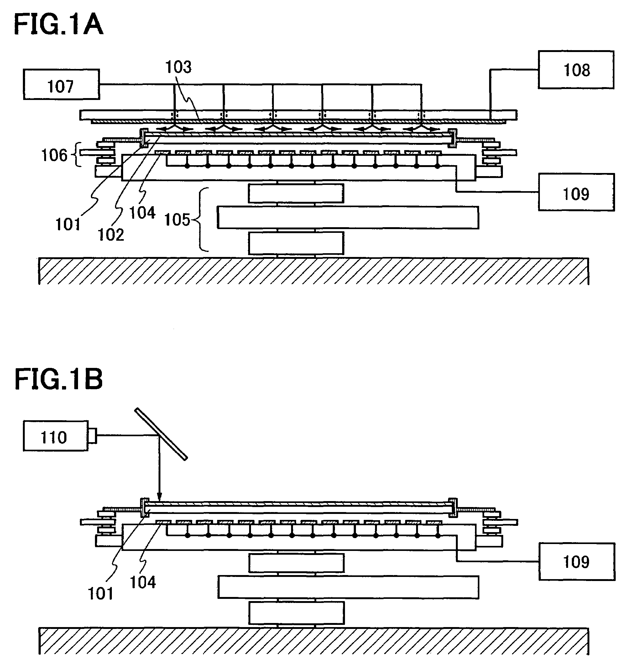
[0075]Embodiment 1 describes a configuration of an inspection system (apparatus) of the present invention more concretely with reference to FIG. 8.

[0076]The inspection system (apparatus) of this embodiment shown in FIG. 8 includes a plurality of inspection electrodes 801, a plurality of inspection antennas 802, a position control unit (means for controlling a position, an alignment apparatus) 803, a voltage supply unit (means for supplying a voltage, a voltage apply apparatus) 804 for applying voltage to each of the plurality of inspection antennas 802, and a potential measuring unit (means for measuring potential, a potentials measuring apparatus) 805 for measuring potentials of the plurality of inspection electrodes 801. The inspection system (apparatus) of this embodiment also includes a unit (analyzing unit, means) 806 for analyzing data having potentials of the plurality of inspection electrodes 801 measured by the potential measuring unit 805 as information and data having pos...

embodiment 2

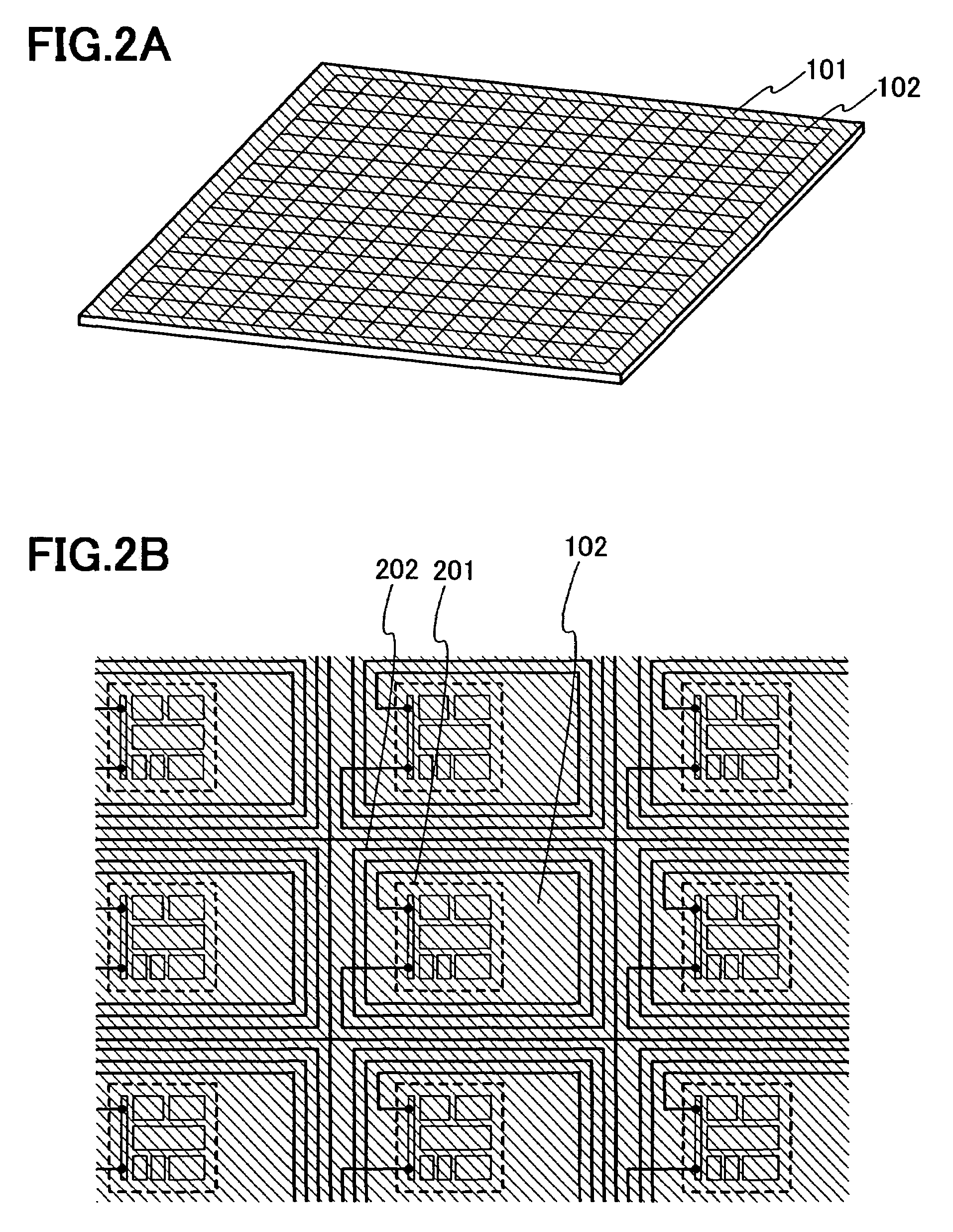
[0089]Embodiment 2 describes one mode of a functional configuration / structure of an ID chip according to the present invention with reference to FIG. 9.

[0090]In FIG. 9, reference numeral 900 denotes an antenna, and 901 denotes an integrated circuit. The antenna 900 comprises an antenna coil 902 and a capacitor element 903 formed within the antenna coil 902. The integrated circuit 901 comprises a demodulation circuit 909, a modulation circuit 904, a rectification circuit 905, a microprocessor 906, a memory 907, and a switch 908 for providing load modulation to the antenna 900. In addition, the number of the memory 907 is not limited to one; a plurality of the memories 907 may be provided. As the memory 907, an SRAM, a flash memory, a ROM, an FRAM (registered mark), or the like may be used.

[0091]A signal sent from the reader / writer as radio wave is converted into an alternating electric signal by electromagnetic induction in the antenna coil 902. The alternating electric signal is dem...

embodiment 3

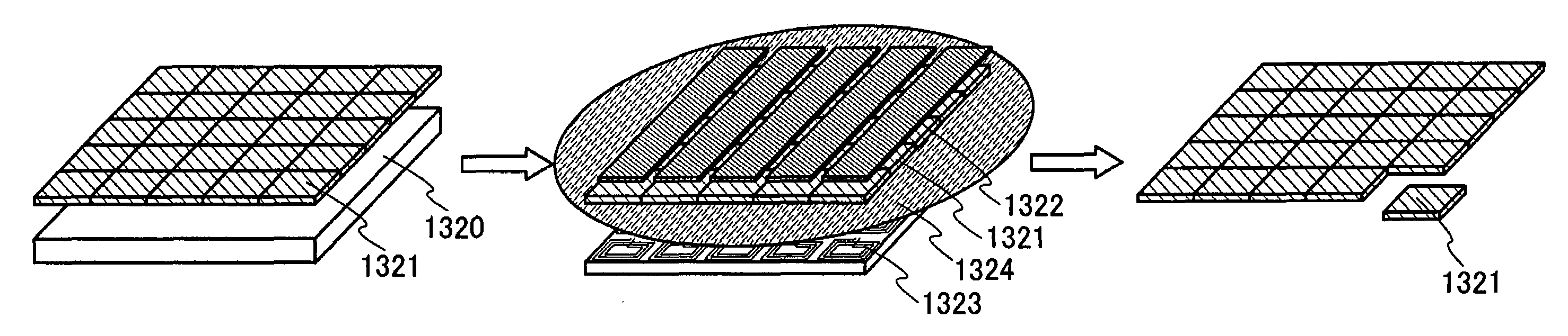
[0095]Next, timing of conducting an inspection according to the present invention in a manufacturing process of an ID chip is described. Note that a TFT that is insulated as a semiconductor element is described as an example in this embodiment, but semiconductor elements included in an integrated circuit are not limited to this and various types of circuit elements can be used. A memory element, a diode, a photoelectric conversion element, a resistor element, a coil, a capacitor element, an inductor and the like can be given as a representative example in addition to a TFT.

[0096]As shown in FIG. 10A, a separation layer 501 is formed on a substrate 500 by a sputtering method. A glass substrate such as a barium borosilicate glass or an alumino borosilicate glass, or the like that can resist processing temperature in a later manufacturing step and that prevents radio waves worse than a semiconductor substrate in an inspection step is used as the substrate 500.

[0097]A layer mainly conta...


PUM


Abstract

The present invention provides an inspection system of ID chips that can supply a signal or power supply voltage to an ID chip without contact, and can increase throughput of an inspection process and an inspection method using the inspection system. The inspection system according to the present invention includes a plurality of inspection electrodes, a plurality of inspection antennas, a position control unit, a unit for applying voltage to each of the inspection antennas, and a unit for measuring potentials of the inspection electrodes. One feature of the inspection system is that a plurality of ID chips and the plurality of inspection electrodes are overlapped with a certain space therebetween, and the plurality of ID chips and the plurality of inspection antennas are overlapped with a certain space therebetween, and the plurality of ID chips are interposed between the plurality of inspection electrodes and the plurality of inspection antennas by the position control unit.

Description

BACKGROUND OF THE INVENTION[0001]1. Field of the Invention[0002]The present invention relates to an inspection system (apparatus), and an inspection method of an ID chip that can conduct communication wirelessly, and method for manufacturing a semiconductor device using said inspection method.[0003]2. Description of the Related Art[0004]A semiconductor device typified by an ID chip that can transmit and receive data such as identification information wirelessly has been put into practice in various areas, and the expansion of its market is further anticipated as a communication information terminal of a new mode. An ID chip is called also a wireless tag, a RFID (Radio frequency identification) tag or an IC tag, and one having an integrated circuit (IC chip) formed by using an antenna and a semiconductor substrate is put to practical use at present.[0005]An ID chip is formed through various manufacturing processes and an inspection process is conducted in the end stage of the manufac...

Claims


Application Information

Patent Timeline
Patent Type & Authority Patents(United States)
IPC IPC(8): H01L21/00H01L21/66H01L21/84G01R31/28G01R31/303
CPCG01R31/2886G01R31/2889G06K7/0095G01R31/3025G01R31/303H01L22/00
Inventor ARAI, YASUYUKITACHIMURA, YUKOAKIBA, MAI
Owner SEMICON ENERGY LAB CO LTD
Why Eureka
Try Eureka