Offset-reduced hall sensor

a hall sensor and offset reduction technology, applied in the field of magnetic field sensors, can solve the problems of inability to adjust the offset drift of the hall sensor, and the properties of the currently known vertical sensor are often very inaccura

Active Publication Date: 2006-10-10
TDK MICRONAS GMBH
View PDF9 Cites 66 Cited by
  • Summary
  • Abstract
  • Description
  • Claims
  • Application Information

AI Technical Summary

Benefits of technology

[0009]In an advantageous approach, not only the position of the current feed points is spatially displaced, but so too is the position of the taps to tap the Hall voltage. One embodiment, during the first measurement of the available five taps, of which the two outer ones are combined, are employed to feed in or feed out the Hall sensor current, or to tap the Hall voltage with offset. In the second measurement, the terminals for the current in-feed and out-feed, and for tapping the Hall voltage, are transposed. As a result, a simple switching of the terminals—which may be implemented by a mechanical or electronic switch—can generate a current flow situation analogous to that found in a known bridge circuit. An especially advantageous aspect here is that the repeated displacement in a second direction, or in the case of the bridge circuit, simply the additional reversal of the current and repeated implementation of the two measurements, may be exploited such that ultimately four individual Hall voltages with offset are determined which may be used to compensate the offset or offset voltage, and to output an offset-free voltage.

Problems solved by technology

As a result, Hall sensors of this type are susceptible to offset drifts that may occur in response to changes in temperature and fluctuations in voltage, but which may also occur as a result of mechanical stress which the package, for example, transfers to the chip, or due to other factors.
Due to offset voltages, however, the properties of currently known vertical sensors are often very inaccurate and are thus not considered for many possible applications.

Method used


Image

  • Offset-reduced hall sensor
  • Offset-reduced hall sensor
  • Offset-reduced hall sensor

Examples


Embodiment Construction

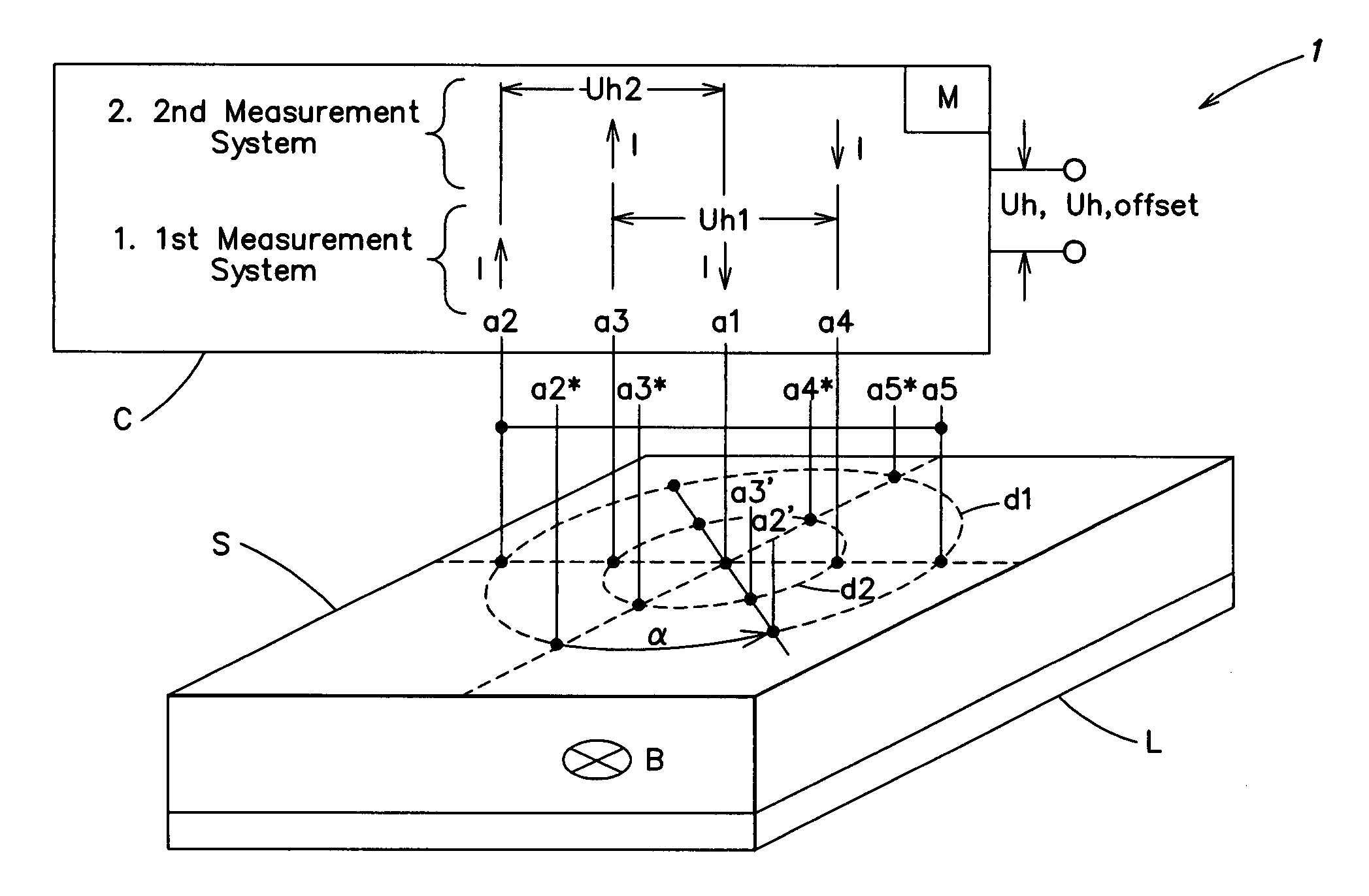
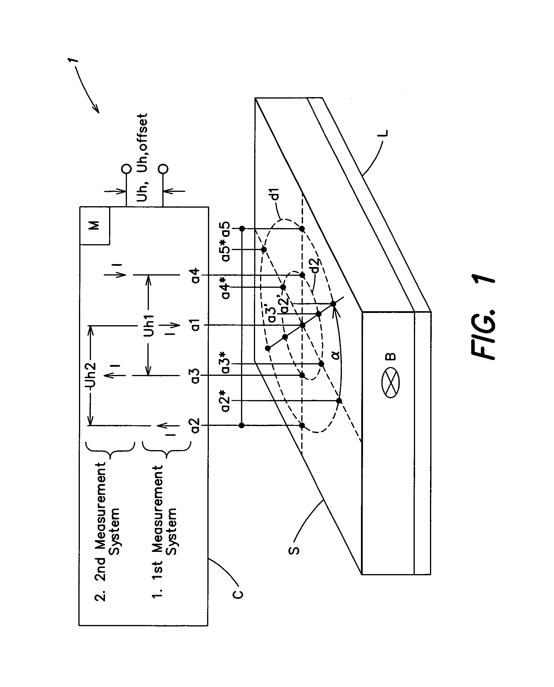
[0020]FIG. 1 illustrates an embodiment of a vertical Hall sensor. This sensor is preferably an integral component of an integrated circuit which, in addition to an actual Hall sensor element S, also has an electronic analyzer in the form of a control circuit C. The actual Hall sensor element is composed of a planar sensor wafer through which flows a magnetic field B. A plurality of taps a1–a5, a2*–a5*, a2′, a3′ are located on one of the planar surfaces of Hall sensor element S. When a corresponding voltage is applied through these taps, an in-feed or out-feed of a Hall sensor current I occurs, as does the tapping of a Hall voltage Uh1, Uh2. In the embodiment shown, a base material or terminating material, such as a conducting layer L, is applied to the surface of Hall sensor element S opposite taps a1, a2, . . . .

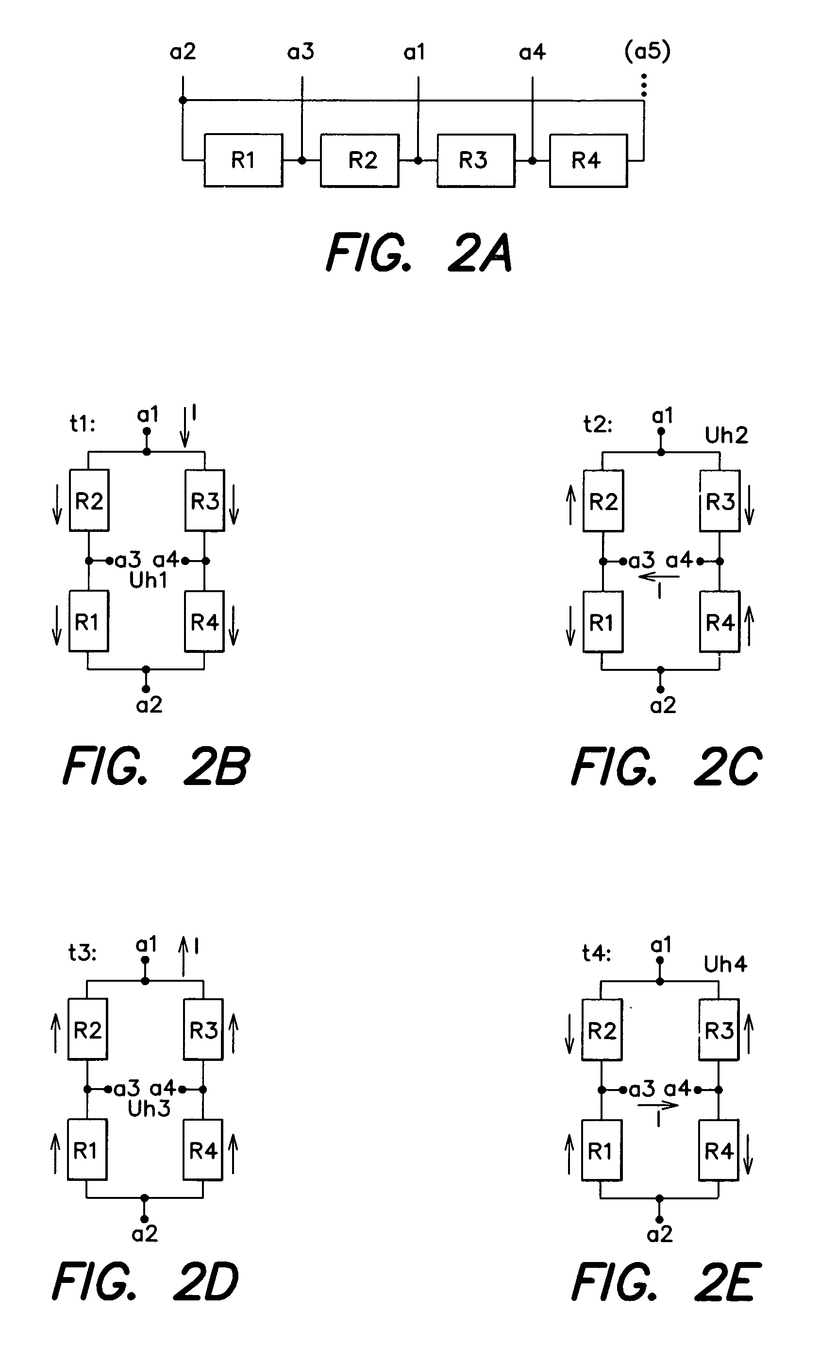
[0021]In a first measurement system, the control circuit C serves to feed Hall sensor current I to the first central tap a1, and feed the current out through the two taps a...


PUM


Abstract

A technique for determining an offset-reduced Hall voltage (Uh), and / or an offset voltage (UH, offset) of a Hall sensor (1) includes applying a Hall sensor current (I) at first and second taps (a1, a2, a3) of the Hall sensor (1), and determining a first Hall voltage (Uh1) at third and fourth taps (a3, a4) displaced from the first and second taps (a1, a2, a5). A second Hall sensor current is applied modified relative to the first, and a second Hall voltage (Uh2) is determined. The Hall voltage (Uh) and / or Hall voltage offset (Uh,offset) are determined from the first and second Hall voltages. To compensate any offset present, a second measurement applies the second Hall sensor current I at taps (a3, a4) that are spatially displaced relative to the first and / or second taps.

Description

BACKGROUND OF THE INVENTION[0001]The present invention relates to the field of magnetic field sensors, and in particular to an offset-compensated Hall sensor.[0002]The publication “Auto & Elektronik” dated 4 / 2000, pages 19–23, discloses a Hall sensor that includes a complete integrated system, including the actual Hall sensor. The area of application is designed for the voltage range 100 μV–1 mV at magnetic field strengths of 2–20 mT. As a result, Hall sensors of this type are susceptible to offset drifts that may occur in response to changes in temperature and fluctuations in voltage, but which may also occur as a result of mechanical stress which the package, for example, transfers to the chip, or due to other factors. To reduce this offset, a so-called chopper method is provided, also known as the “zero-drift principle.” In this method, the current direction of the Hall current through the Hall plate forming the actual sensor element is continually switched. Any corruptions in th...

Claims


Application Information

Patent Timeline
Patent Type & Authority Patents(United States)
IPC IPC(8): G01R33/07H01L43/06G01D5/14
CPCG01D5/145G01D5/147
Inventor BLOSSFELD, LOTHAR
Owner TDK MICRONAS GMBH
Why Eureka
Try Eureka