Back-bias voltage regulator having temperature and process variation compensation and related method of regulating a back-bias voltage

a voltage regulator and temperature and process variation technology, applied in the direction of pulse technique, electric pulse generator details, instruments, etc., can solve the problems of increasing difficulty in providing, leakage current through transistors, and typical increase of leakage curren

Inactive Publication Date: 2006-10-10
TAIWAN SEMICON MFG CO LTD
View PDF7 Cites 41 Cited by
  • Summary
  • Abstract
  • Description
  • Claims
  • Application Information

AI Technical Summary

Problems solved by technology

Many applications implemented on modern semiconductor integrated circuit (IC) chips require accurate operation, which becomes increasingly difficult to provide as chip density continues to increase.
Among the specific problems that can occur in electrical circuits, particularly semiconductor circuitry, is leakage current through the transistors.
As is well known, as the threshold voltage in a metal-oxide-semiconductor field-effect transistor (MOSFET) decreases, leakage current typically increases.
Among the more common causes for a decrease in desired threshold voltage is an increase in temperature or process variations during the manufacturing process for the MOSFET that resulted in a lower threshold voltage than intended or desired.
Early approaches implemented a string of diodes coupled to the MOSFETs to decrease the leakage current, but this approach suffered several disadvantages.
A primary disadvantage was a reduced back-bias voltage as the threshold voltage continued to decrease, which in the end resulted in more leakage current.
Unfortunately, even this approach suffers from disadvantages, particularly the use of a fixed reference voltage on which the regulation of the back-bias voltage is based.

Method used


Image

  • Back-bias voltage regulator having temperature and process variation compensation and related method of regulating a back-bias voltage
  • Back-bias voltage regulator having temperature and process variation compensation and related method of regulating a back-bias voltage
  • Back-bias voltage regulator having temperature and process variation compensation and related method of regulating a back-bias voltage

Examples


Embodiment Construction

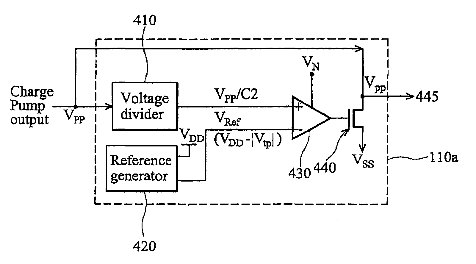
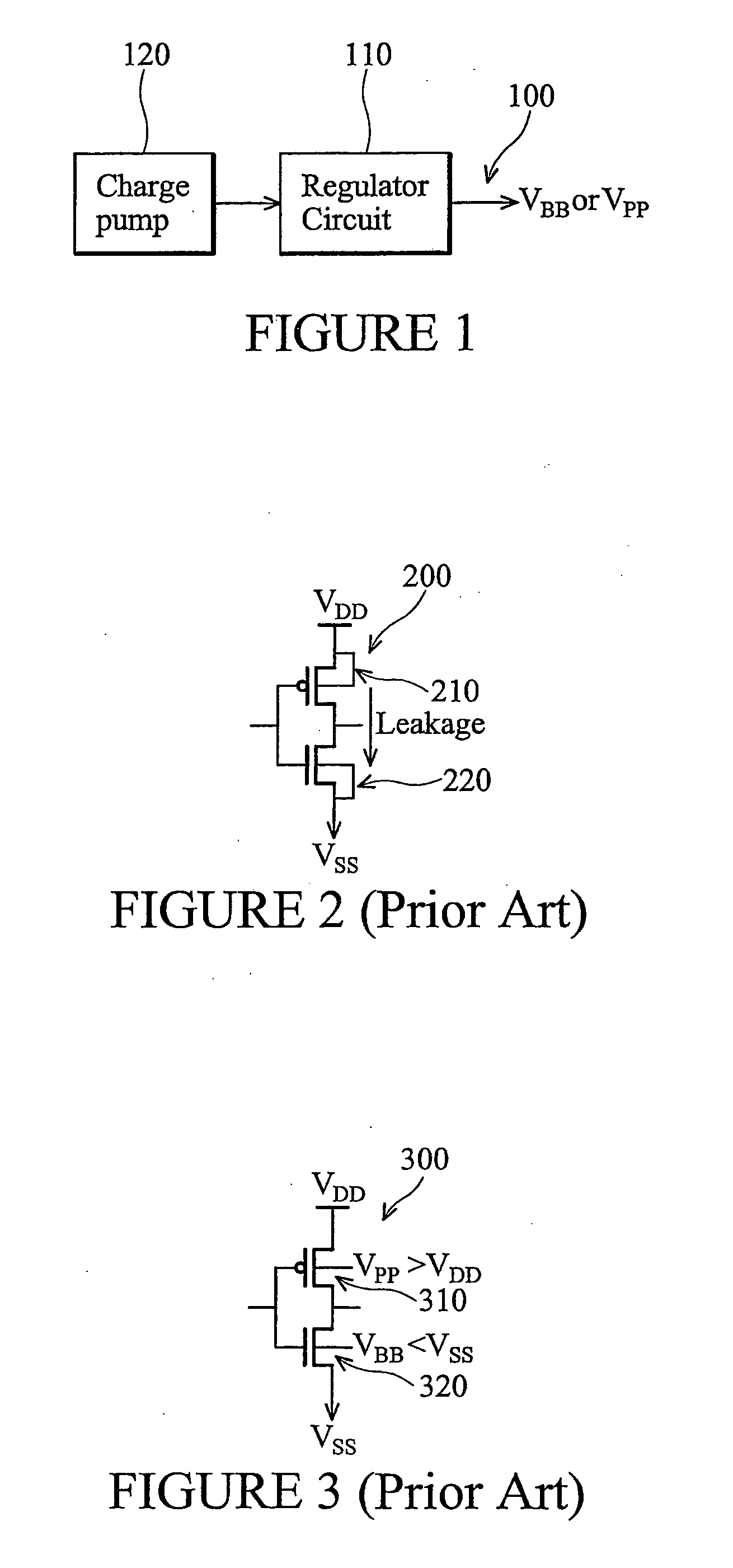
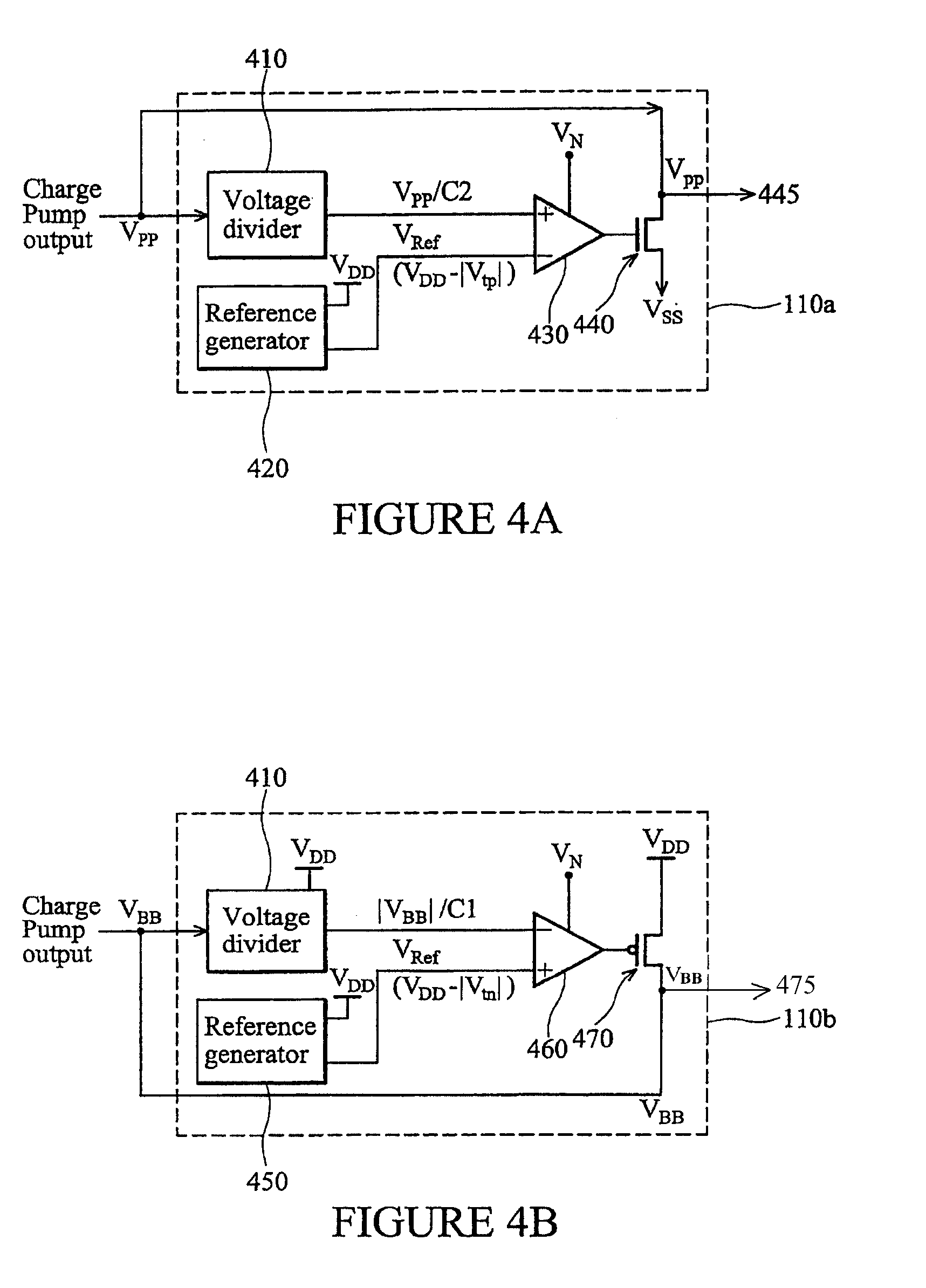
[0018]Referring initially to FIG. 1, illustrated is a general block diagram 100 of a typical environment for a conventional back-bias voltage regulator circuit or a back-bias voltage regulator circuit 110 of the type disclosed herein. As illustrated, such voltage regulators 110 output a back-bias voltage (VPP / VBB), typically based on an input from a charge pump 120. More specifically, the back-bias voltage VPP / VBB is employed to reduce the current leakage typically present across metal-oxide-semiconductor (MOS) devices employed at an operating voltage that is too low or too high, as shown in FIG. 2.

[0019]Looking briefly at FIG. 2, illustrated is a conventional CMOS primary circuit 200 in need of back-bias voltage provided by a regulator circuit, such as the one illustrated in FIG. 1. The CMOS design is provided by a PMOS device 210 and an NMOS device 220. In this conventional layout, no back-bias voltage is applied to the circuit 200 during operation. As a result, a leakage current ...


PUM


Abstract

Disclosed herein is a back-bias voltage regulator circuit for regulating a back-bias voltage used to control leakage current in at least one transistor within a primary circuit. In one embodiment, the back-bias voltage regulator circuit includes a voltage divider circuit configured to receive a back-bias voltage from a charge pump, and to generate a divided voltage signal by dividing the back-bias voltage based on a ratio of resistances of resistive elements within the voltage divider. In addition, the regulator circuit includes an output circuit configured to receive the back-bias voltage from the charge pump and having an output node for outputting the back-bias voltage, as well as a reference voltage circuit configured to generate a reference voltage signal based on a threshold voltage of the at least one transistor in the primary circuit. Also in such an embodiment, the regulator circuit includes a comparison circuit configured to compare the divided voltage signal to the reference voltage signal and to operate the output circuit to regulate the back-bias voltage level based on the comparison. Also disclosed is a related method of regulating a back-bias voltage to control leakage current in at least one transistor within a primary circuit.

Description

TECHNICAL FIELD[0001]Disclosed embodiments herein relate generally to generating and regulating back-bias voltage, and more particularly to a back-bias voltage regulator circuit for regulating a back-bias voltage in response to temperature and / or process variations.BACKGROUND[0002]In recent years, there continues to be dramatic density increases in integrated circuit technology for semiconductor chips. For example, the minimum feature size of lithography, such as the size of MOSFETs, has presently been reduced to one micrometer and below. Many applications implemented on modern semiconductor integrated circuit (IC) chips require accurate operation, which becomes increasingly difficult to provide as chip density continues to increase.[0003]Among the specific problems that can occur in electrical circuits, particularly semiconductor circuitry, is leakage current through the transistors. As is well known, as the threshold voltage in a metal-oxide-semiconductor field-effect transistor (...

Claims


Application Information

Patent Timeline
Patent Type & Authority Patents(United States)
IPC IPC(8): H03K3/01G05F1/10G05F3/20
CPCG05F3/205H03K2217/0018
Inventor CHIH, YUE-DER
Owner TAIWAN SEMICON MFG CO LTD
Why Eureka
Try Eureka