
Individually adjustable back-bias technique

a back bias and individual adjustment technology, applied in pulse technique, radiation control device, transistor, etc., can solve the problems of significant impact on performance and power consumption, significant influence of die-to-die and within-die variations, and silicon manufacturers have not been able to keep up with technology scaling, so as to achieve close control of chip power and performance, the effect of reducing the effect of d2d and wd process variations

Inactive Publication Date: 2005-02-22
HEWLETT PACKARD DEV CO LP
View PDF3 Cites 26 Cited by
  • Summary
  • Abstract
  • Description
  • Claims
  • Application Information

AI Technical Summary

Benefits of technology

An individual-well adaptive method of body bias control (IW ABB) that mitigates the effects of D2D and WD process variations is shown. It is assumed that p-type transistors are grouped in sections. The bodies of all the p-type transistors within a section are connected to a single n-well. This section size can be small enough to provide fine-granular adjustments to the circuit without having any impact on area overhead. With a small amount of additional circuitry and routing, individual well biases can be intelligently adjusted resulting in closely controlled chip power and performance. Experimental results show that binning yields as low as 17% can be improved to greater than 90% using the proposed method.

Problems solved by technology

As modern CMOS technology is scaled down, the effects of die-to-die and within-die variations are becoming worse.
For high performance VLSI chips, die-to-die and within-die variations have a significant impact on their performance and power consumption.
Even though significant advances have been made to reduce process variations, silicon manufacturers have not been able to keep up with technology scaling.
These large relative variations cause wide distributions of circuit operating frequencies and power dissipation.
Results suggest that, while the simplest implementation of ABB was effective in mitigating the effects of die-to-die (D2D) variation, its effect on within-die (WD) variation was limited.
The effectiveness of this method is further limited by the size of the sections used.
This proves to be enormously expensive in both die area and routing resources.
Also, localized areas of high variations within a section are not addressed.

Method used


Image

  • Individually adjustable back-bias technique
  • Individually adjustable back-bias technique
  • Individually adjustable back-bias technique

Examples


Embodiment Construction

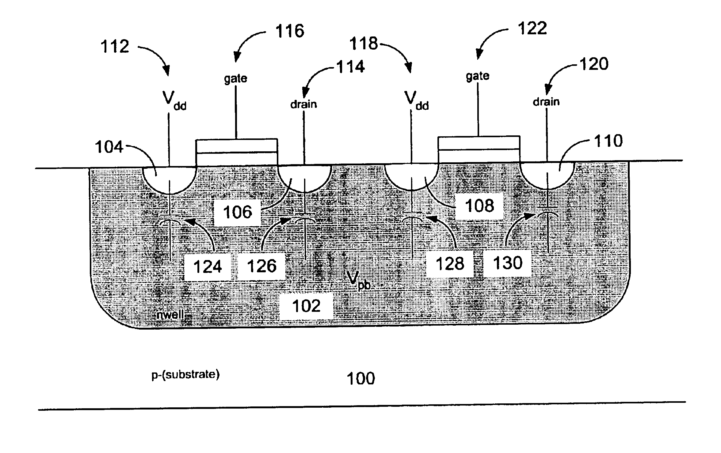
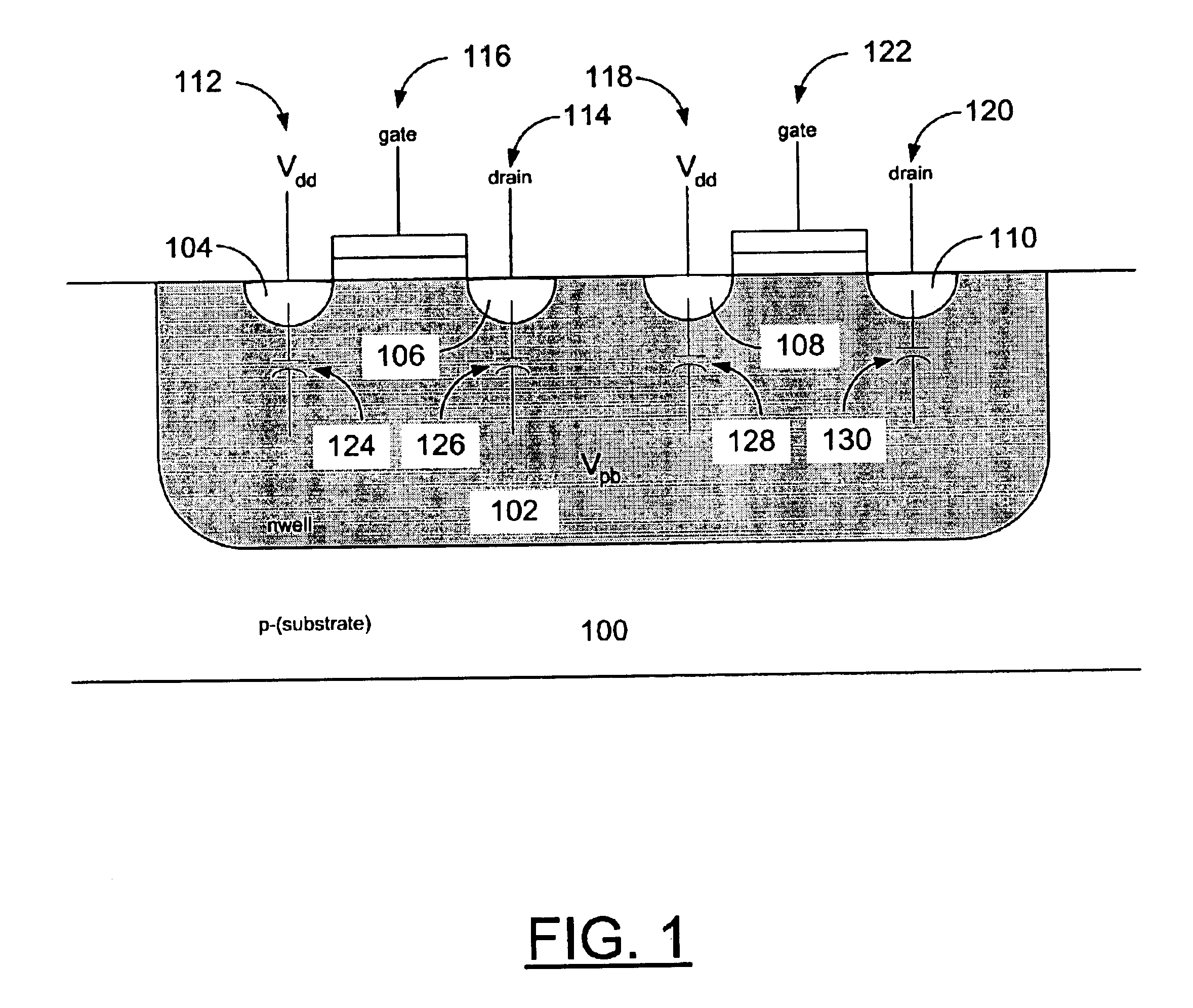
In an n-well or triple-well CMOS process, n-wells (pfet bodies) are normally connected directly to the power supply voltage, Vdd. Reducing the pfet body bias reduces their threshold voltage, Vt, making the pfets switch faster and increasing their leakage current. Since pfets are inherently slower than nfets, their switching speed is usually one of the limiting factors in overall circuit performance. Increasing pfet speed can provide a significant speed up of the entire circuit. However, instead of using a separate power supply and power grid to control Vpb (the body voltage of the pfets) as previous researchers have done, one can use the capacitive coupling between drain and body of the pfets to provide Vpb for an entire n-well as illustrated in FIG. 1.

FIG. 1 is a cross-sectional view of an n-well including two pfets. In the example embodiment of the present invention shown in FIG. 1, an n-well 102 is created within a p-substrate 100. Two pfets are shown. A first pfet includes a fir...


PUM


Abstract

An individual-well adaptive method of body bias control that mitigates the effects of D2D and WD process variations is shown. It is assumed that p-type transistors are grouped in sections. The bodies of all the p-type transistors within a section are connected to a single n-well. This section size can be small enough to provide fine-granular adjustments to the circuit without having any impact on area overhead. With a small amount of additional circuitry and routing, individual well biases can be intelligently adjusted resulting in closely controlled chip power and performance. Experimental results show that binning yields as low as 17% can be improved to greater than 90% using the proposed method.

Description

FIELD OF THE INVENTIONThe present invention relates generally to the field of integrated circuits and more specifically to the field of minimization of the effects of die-to-die (D2D) and within-die (WD) process variations within integrated circuits.BACKGROUND OF THE INVENTIONAs modern CMOS technology is scaled down, the effects of die-to-die and within-die variations are becoming worse. Process variations can be categorized into four tiers, lot-to-lot variations, wafer-to-wafer variations, die-to-die variations, and within-die variations. For high performance VLSI chips, die-to-die and within-die variations have a significant impact on their performance and power consumption. Even though significant advances have been made to reduce process variations, silicon manufacturers have not been able to keep up with technology scaling. An existing statistical model, assuming a 3σ channel length deviation of 20% for the 50-nm technology generations, indicates that essentially a generation o...

Claims


Application Information

Patent Timeline
Patent Type & Authority Patents(United States)
IPC IPC(8): H01L21/70H01L21/8238H01L27/085H01L27/092H01L21/822H01L27/04H03K19/096
CPCH01L21/823892H01L29/7841H01L27/0925
Inventor CHEN, THOMAS W.
Owner HEWLETT PACKARD DEV CO LP
Learn More