Coupled body contacts for SOI differential circuits

a differential circuit and coupling body technology, applied in the field of very large-scale integrated circuits, can solve the problems of non-uniformity of devices, increased wiring difficulty of circuits, and increased risk of localized device phenomena known as body effects

Inactive Publication Date: 2005-03-15
GLOBALFOUNDRIES US INC
View PDF3 Cites 28 Cited by
  • Summary
  • Abstract
  • Description
  • Claims
  • Application Information

AI Technical Summary

Benefits of technology

The present invention relates to a silicon on insulator (SOI) CMOS circuit, macro and integrated circuit (IC) chip. The chip or macro may include be an SRAM in partially depleted (PD) SOI CMOS. Most field effect transistors (FETs) do not have body contacts. FETs otherwise exhibiting a sensitivity to history effects have body contacts. The body contact for each such FET is connected to at least one other body contact. A back bias voltage may be provided to selected FETs.

Problems solved by technology

Back biases may be applied to SOI FETs through a contact to the underlying layer (or body contact) that may require as much area as the FET itself and may make circuit wiring more difficult.
Unfortunately, as body contacts are eliminated or at the very least shared by more and more devices, individual devices become much more susceptible to localized device phenomena known as body effects.
Localized body effect variations cause device non-uniformity.
Device leakage and parasitic bipolar effects may add to the charge.
So, body effects may cause two devices that are identical by design may exhibit some difference, difference that may be time varying from changing circuit conditions.
These localized body effects and other sporadically occurring parasitic bipolar effects, i.e., at source / drain diffusion junctions, are serious design problems for densely packed SOI circuits such as for example, memory arrays, e.g., a Static RAM (SRAM) macro.
However, repetitively accessing RAM cells, both to read and to write, unintentionally induces local body effects in some cell devices.
These local effects can cause the SRAM cell to favor one state over the other, resulting in sporadic read upsets with no apparent reason.
An imbalance in cell pass gates may increase cell write time and sense time.
As a result, intermittent problems may arise, such as spuriously reading the wrong data or, random cell failures.
These types of intermittent problems are notoriously difficult to identify and diagnose.
So, channel bias variations from body effects causes device non-uniformities that result in difficult to identify sporadic chip failures sometimes characterized as “soft failures.”
Dynamic circuits are Especially sensitive to such process variations which can result in inter or intra macro timing problems, race conditions, high leakage / power and reduced noise margins.
Consequently, such chips, macros and other circuits with threshold variation sensitivities, either have performance and reliability below what it might be with back biased devices or, are larger (and so, more expensive) than they might otherwise be if body contacts were not included.

Method used


Image

  • Coupled body contacts for SOI differential circuits
  • Coupled body contacts for SOI differential circuits
  • Coupled body contacts for SOI differential circuits

Examples


Embodiment Construction

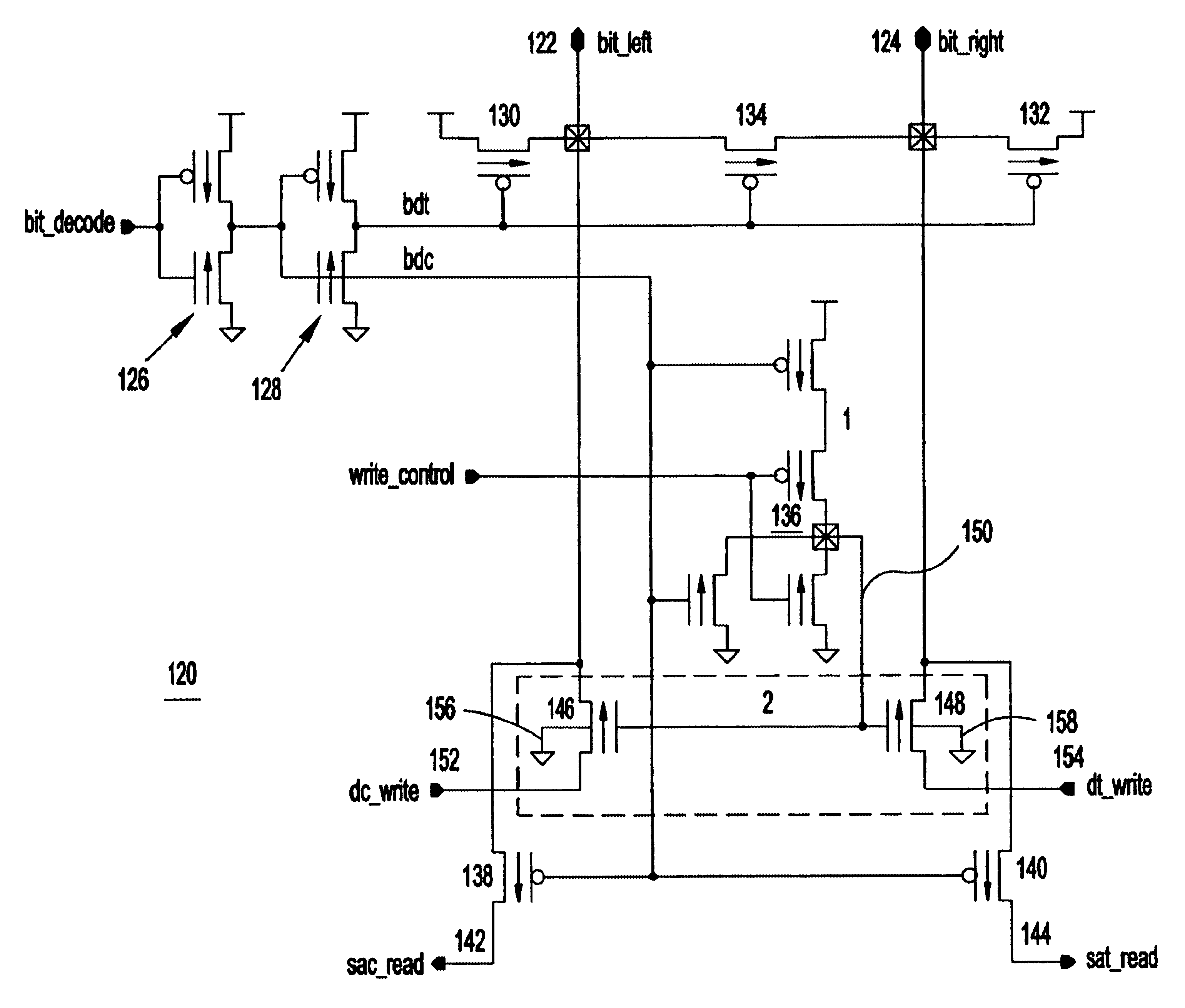
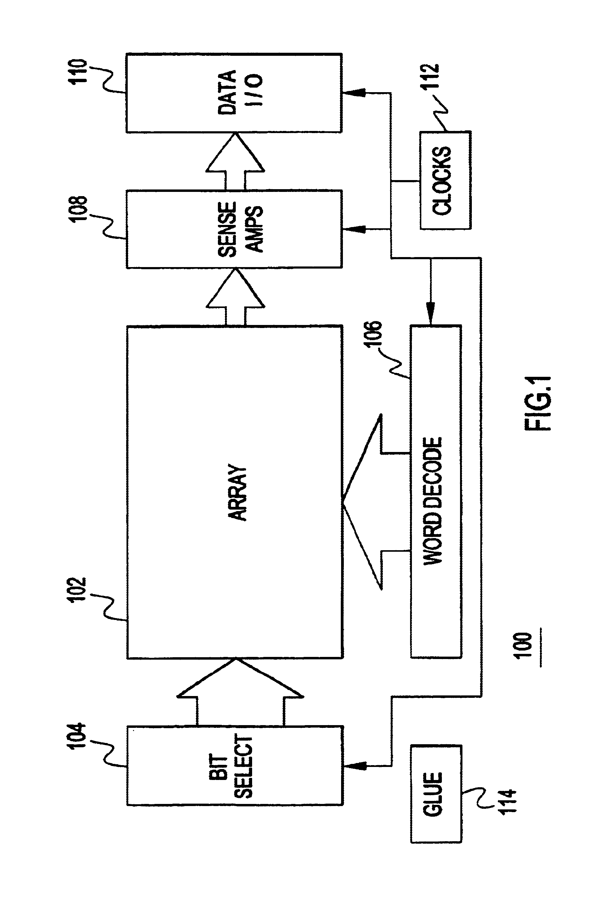
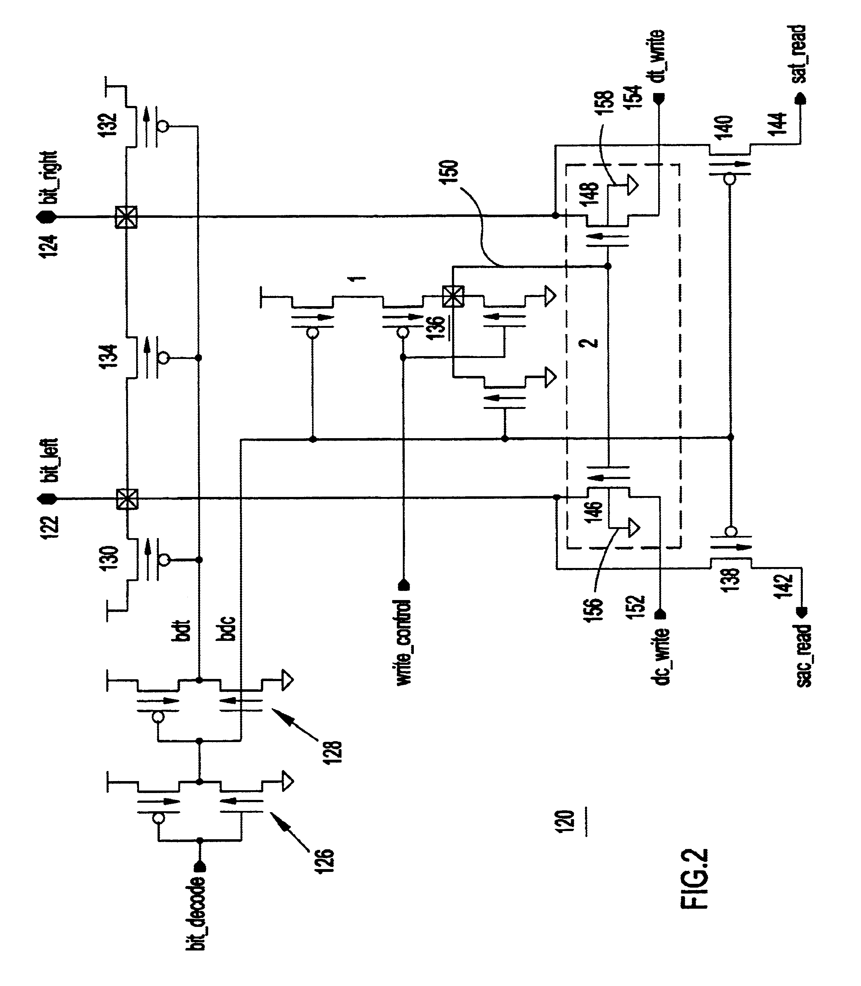
Referring now to the drawings, and more particularly, FIG. 1 shows an example of a block diagram of a memory 100, macro or chip, according to a preferred embodiment of the present invention, wherein back bias contacts are provided only to selected devices and, otherwise, not included. In this example, cells (not shown) of an array 102 are selected by coincidence a column selected by bit select circuit 104 with a row selected by word decoder 106. Selected cells are couple to sense amplifiers 108 for reading data stored in cells during a read. Data from the sense amplifiers 108 are passed to data input / output (I / O) drivers 110. Body contacts are provided only for selected devices, e.g., in each of the bit select 104 and the sense amplifiers 106. Clock logic 112 provides local timing and glue logic 114 provides local control logic. Optionally, selected devices can be identified in each of the remaining circuits, including word decode 108, clocks 112 and glue 114. Typically, however, de...


PUM


Abstract

A silicon on insulator (SOI) CMOS circuit, macro and integrated circuit (IC) chip. The chip or macro may include be an SRAM in partially depleted (PD) SOI CMOS. Most field effect transistors (FETs) do not have body contacts. FETs otherwise exhibiting a sensitivity to history effects have body contacts. The body contact for each such FET is connected to at least one other body contact. A back bias voltage may be provided to selected FETs.

Description

FIELD OF THE INVENTIONThe present invention relates to semiconductor integrated circuit and, more particularly to very large scale integrated (VLSI) circuits wherein field effect transistors (FETs) are formed in a surface layer of a silicon on insulator (SOI) chip.BACKGROUND DESCRIPTIONBulk silicon field effect transistors (FETs) are formed on the surface of a silicon chip or wafer. In what is typically referred to as CMOS technology, the silicon wafer or substrate may be of one conduction type, e.g., P-type, and areas or wells of a second conduction type, e.g., N-type, are formed in the P-type wafer. N-type FETs (NFETs) are formed on the surface of the P-type wafer and P-type FETs (PFETs) are formed on the surface of the N-wells. FET device characteristics, including threshold voltage (Vt) and device currents, are dependent upon device substrate voltage (Vsx). So, typically, a first bias voltage, typically zero Volts (0V) or ground (GND), is applied to the substrate to bias the NFE...

Claims


Application Information

Patent Timeline
Patent Type & Authority Patents(United States)
IPC IPC(8): G11C11/412
CPCG11C11/412
Inventor CHAN, YUEN H.JOSHI, RAJIV V.PELELLA, ANTONIO R.
Owner GLOBALFOUNDRIES US INC
Why Eureka
Try Eureka