Semiconductor device, nonvolatile memory device including the same, electronic system including the same, and method for fabricating the same

a semiconductor device and nonvolatile memory technology, applied in semiconductor devices, electrical devices, instruments, etc., can solve the problems of leakage current and reduced size of components in semiconductor devices

Pending Publication Date: 2022-06-30
SAMSUNG ELECTRONICS CO LTD
View PDF0 Cites 0 Cited by
  • Summary
  • Abstract
  • Description
  • Claims
  • Application Information

AI Technical Summary

Problems solved by technology

As the semiconductor devices (e.g., transistors) are highly integrated, the sizes of components included in the semiconductor devices are reduced, which causes a problem of a leakage current.

Method used


Image

  • Semiconductor device, nonvolatile memory device including the same, electronic system including the same, and method for fabricating the same
  • Semiconductor device, nonvolatile memory device including the same, electronic system including the same, and method for fabricating the same
  • Semiconductor device, nonvolatile memory device including the same, electronic system including the same, and method for fabricating the same

Examples


Embodiment Construction

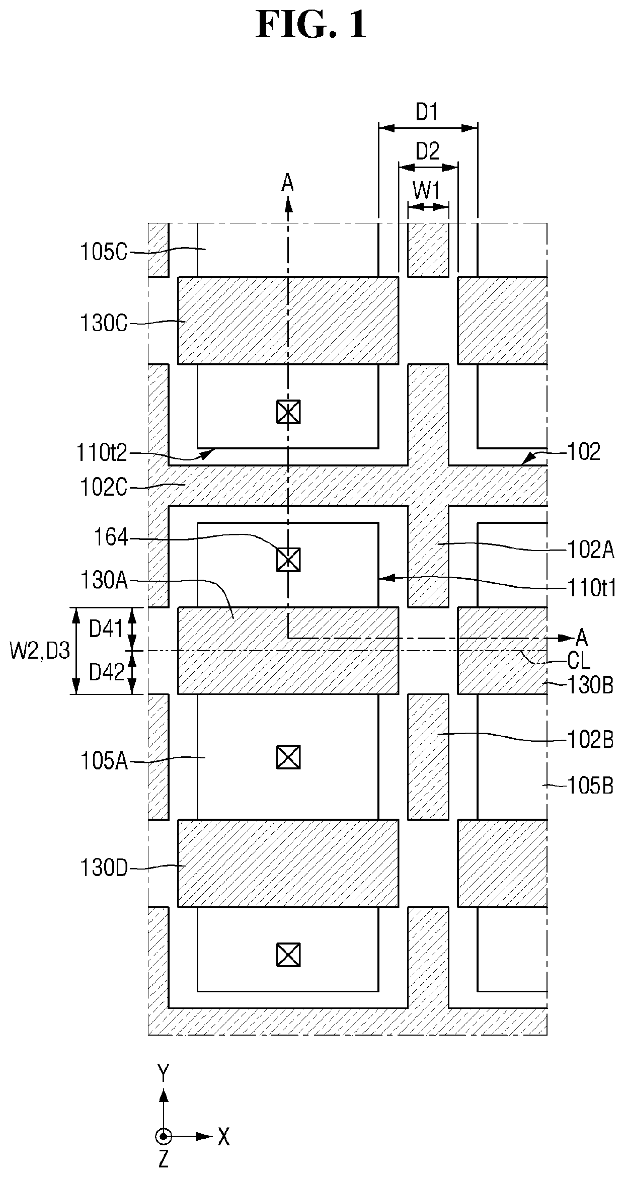
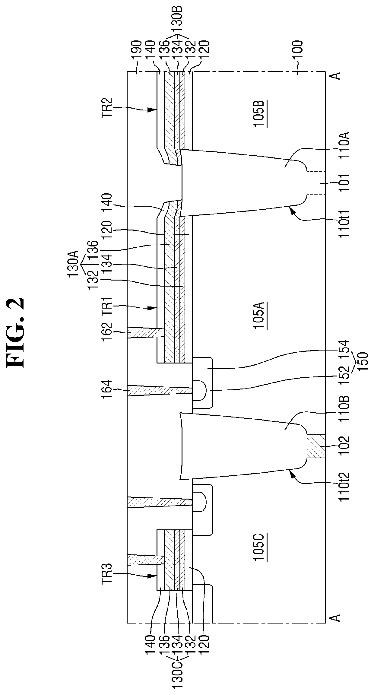
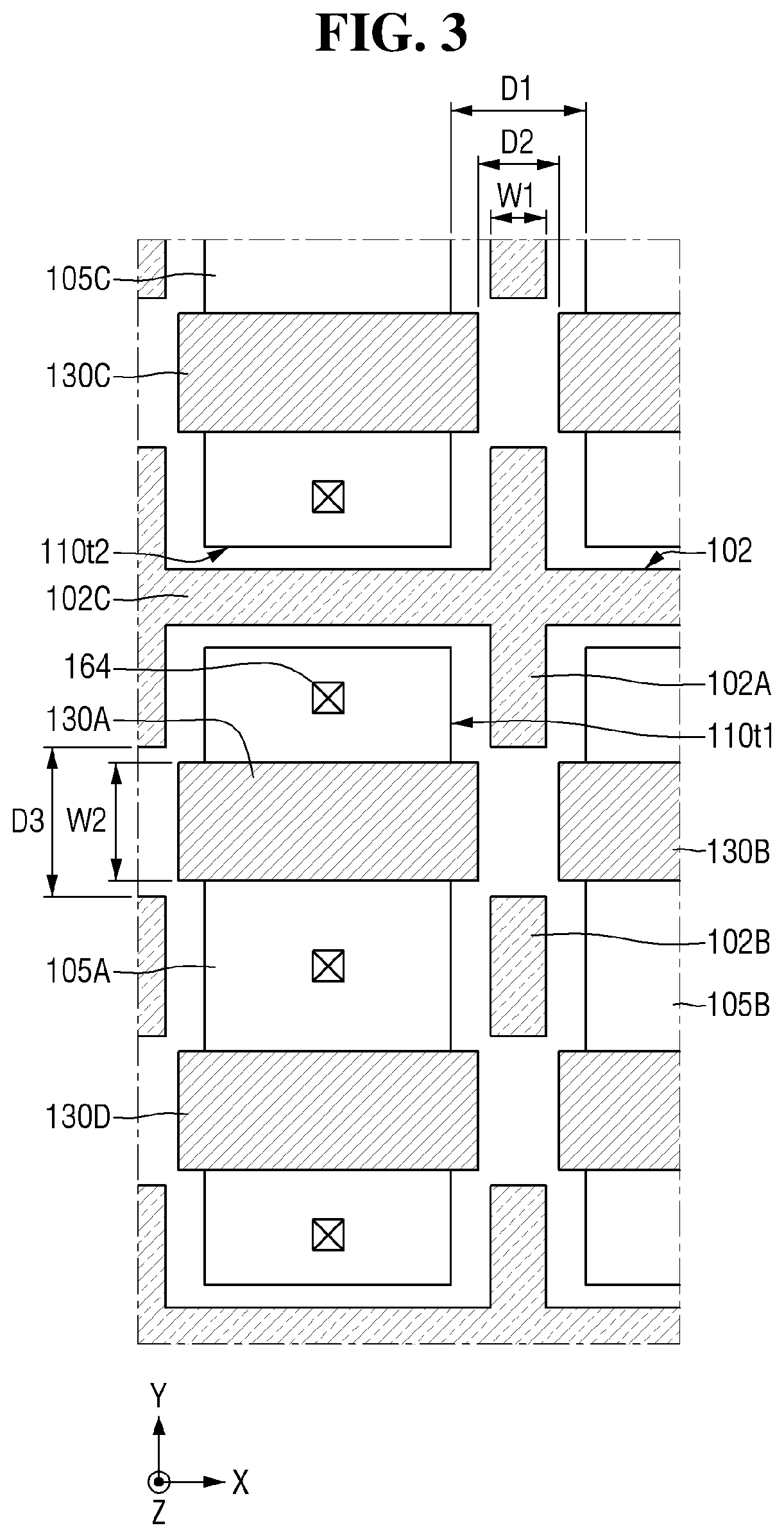
[0030]Hereinafter, a semiconductor device according to an embodiment of the present disclosure will be described with reference to FIGS. 1 to 6.

[0031]FIG. 1 is a layout diagram illustrating a semiconductor device according to an embodiment of the present disclosure. FIG. 2 is a schematic cross-sectional view taken along line A-A of FIG. 1. FIGS. 3 and 4 are various layout diagrams each illustrating a semiconductor device according to an embodiment of the present disclosure.

[0032]Referring to FIGS. 1 to 4, the semiconductor device according to an embodiment of the present disclosure may include a first substrate 100, element isolation layers 110A and 110B, first to third circuit elements TR1, TR2, and TR3, an isolation impurity region 102, an interlayer insulating layer 190, a gate contact 162 and a source / drain contact 164. For simplicity of description, the illustration of the gate contact 162 is omitted in FIG. 1.

[0033]The first substrate 100 may include a base substrate and an ep...


PUM

PropertyMeasurementUnit
voltageaaaaaaaaaa
leakage currentaaaaaaaaaa
conductivityaaaaaaaaaa

Abstract

A semiconductor device includes a first active region and a second active region arranged along a first direction in a substrate, an element isolation layer extending in a second direction in the substrate to isolate the first active region and the second active region, a first gate electrode extending in the first direction on the first active region, a second gate electrode extending in the first direction on the second active region, and an isolation impurity region containing impurities of a first conductivity type in the substrate and disposed below the element isolation layer, in which the isolation impurity region includes a first isolation region and a second isolation region spaced apart from each other in the second direction, and at least a part of the substrate interposed between the first gate electrode and the second gate electrode is interposed between the first isolation region and the second isolation region.

Description

CROSS-REFERENCE TO RELATED APPLICATION[0001]This application claims priority under 35 U.S.C. § 119 to Korean Patent Application No. 10-2020-0185851, filed on Dec. 29, 2020, in the Korean Intellectual Property Office, the contents of which are incorporated by reference herein in their entirety.TECHNICAL FIELD[0002]The present disclosure relates to a semiconductor device, a nonvolatile memory device including the same, an electronic system including the same, and a method for fabricating the same. More particularly, the present disclosure relates to a semiconductor device including an element isolation layer, a nonvolatile memory device including the same, an electronic system including the same, and a method for fabricating the same.DISCUSSION OF RELATED ART[0003]Recently, the trend toward lighter, thinner, shorter and smaller electronic products has resulted in an increasing demand for highly integrated semiconductor devices. As the semiconductor devices (e.g., transistors) are high...

Claims


Application Information

Patent Timeline
Patent Type & Authority Applications(United States)
IPC IPC(8): H01L27/11524H01L27/11519H01L27/11556H01L27/11526G11C5/06H01L29/06
CPCH01L27/11524H01L27/11519H01L29/0649H01L27/11526G11C5/06H01L27/11556H01L21/823481H10B43/40G11C5/063H10B41/50H10B43/50H10B41/27H10B43/27H01L21/823418H01L21/823475H01L21/823462H01L25/0657H01L24/05H10B43/35H10B41/35H10B41/10H10B41/40
Inventor LEE, SO HYUNYUN, KANG-OH
Owner SAMSUNG ELECTRONICS CO LTD
Why Eureka
Try Eureka