Polishing pad having a groove arrangement for reducing slurry consumption

a technology of slurry consumption and polishing pad, which is applied in the direction of grinding machine, manufacturing tools, lapping machines, etc., can solve the problems of high slurry consumption and insufficient utilization of slurry provided to polishing layers

Inactive Publication Date: 2006-10-24
ROHM & HAAS ELECTRONICS MATERIALS CMP HLDG INC
View PDF11 Cites 24 Cited by
  • Summary
  • Abstract
  • Description
  • Claims
  • Application Information

AI Technical Summary

Problems solved by technology

It is generally acknowledged among CMP practitioners that certain groove patterns result in higher slurry consumption than others to achieve comparable material removal rates.
While grooves must be provided with a minimum depth to reliably convey slurry as the surface of the polishing layer wears down, any excess depth will result in some of the slurry provided to polishing layer not being utilized, since in conventional polishing layers an unbroken flow path exists beneath the workpiece wherein the slurry flows without participating in polishing.

Method used


Image

  • Polishing pad having a groove arrangement for reducing slurry consumption
  • Polishing pad having a groove arrangement for reducing slurry consumption
  • Polishing pad having a groove arrangement for reducing slurry consumption

Examples


Embodiment Construction

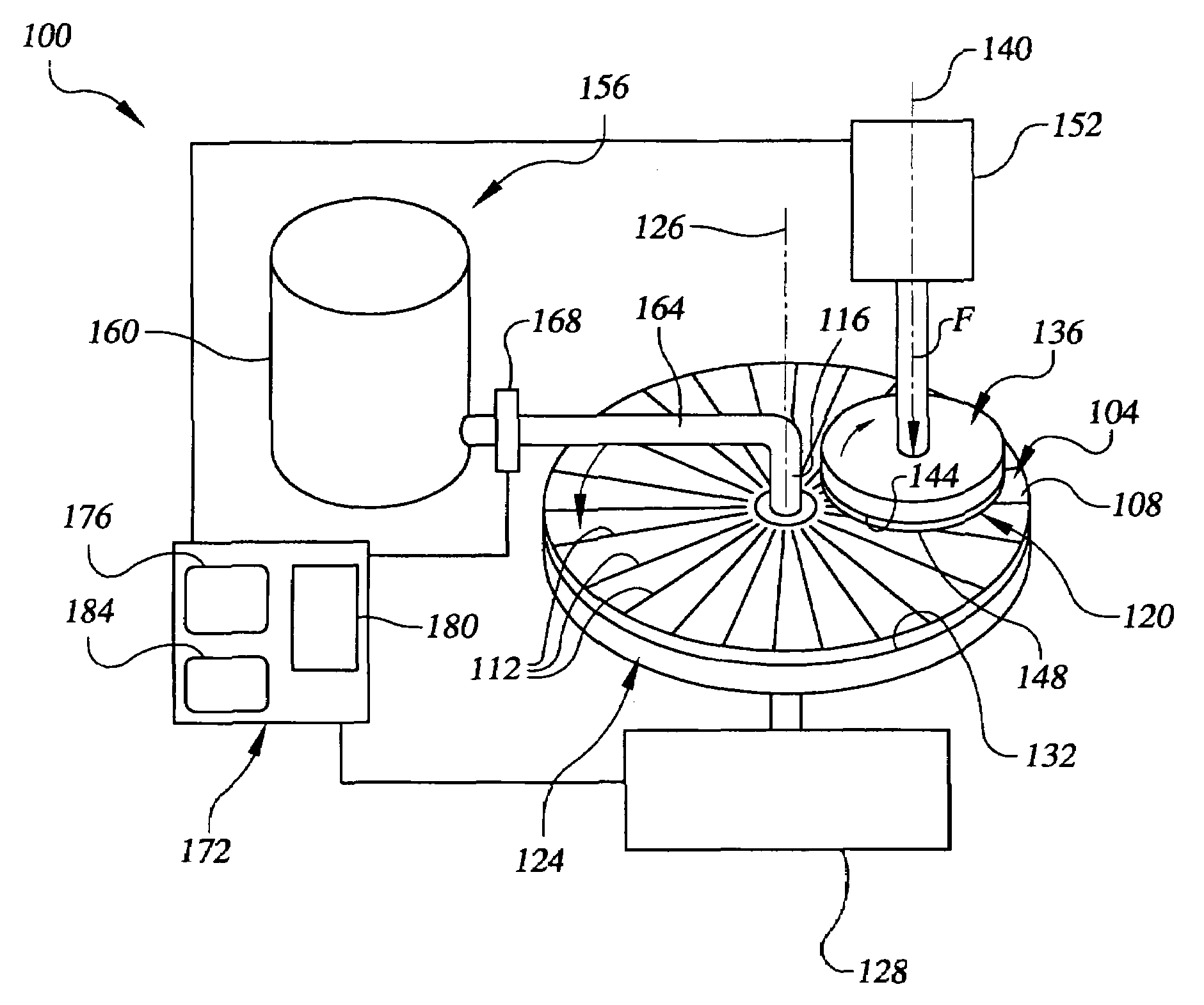
[0017]Referring now to the drawings, FIG. 1 shows in accordance with the present invention a chemical mechanical polishing (CMP) system, which is generally denoted by the numeral 100. CMP system 100 includes a polishing pad 104 having a polishing layer 108 that includes a plurality of grooves 112 arranged and configured for enhancing the utilization of a slurry 116, or other liquid polishing medium, applied to the polishing pad during polishing of a semiconductor substrate, such as semiconductor wafer 120 or other workpiece, such as glass, silicon wafers and magnetic information storage disks, among others. For convenience, the term “wafer” is used in the description below. However, those skilled in the art will appreciate that workpieces other than wafers are within the scope of the present invention. Polishing pad 104 and its unique features are described in detail below.

[0018]CMP system 100 may include a polishing platen 124 rotatable about an axis 126 by a platen driver 128. Pla...


PUM

PropertyMeasurementUnit
pressureaaaaaaaaaa
conductingaaaaaaaaaa
semiconductingaaaaaaaaaa

Abstract

A polishing pad (200) that includes a polishing layer (204) having a polishing region (208) for polishing a wafer (220). The polishing layer includes a set of inflow grooves (232) that extend into the polishing region and a set of outflow grooves (236) that extend out of the polishing region. The inflow and outflow grooves cooperate with one another to enhance the utilization of a polishing slurry during polishing of the wafer.

Description

BACKGROUND OF THE INVENTION[0001]The present invention generally relates to the field of chemical mechanical polishing. More particularly, the present invention is directed to a polishing pad having a groove arrangement for reducing slurry consumption.[0002]In the fabrication of integrated circuits and other electronic devices, multiple layers of conducting, semiconducting and dielectric materials are deposited onto or removed from a surface of a semiconductor wafer. Thin layers of conducting, semiconducting and dielectric materials may be deposited by a number of deposition techniques. Common deposition techniques in modern wafer processing include physical vapor deposition (PVD), also known as sputtering, chemical vapor deposition (CVD), plasma-enhanced chemical vapor deposition (PECVD) and electrochemical plating. Common removal techniques include wet and dry isotropic and anisotropic etching, among others.[0003]As layers of materials are sequentially deposited and removed, the u...

Claims


Application Information

Patent Timeline
Patent Type & Authority Patents(United States)
IPC IPC(8): B24B1/00B24B5/00B24B37/00B24B21/00B24B37/04H01L21/304
CPCB24B37/26B24B21/00H01L21/304
Inventor MULDOWNEY, GREGORY P.
Owner ROHM & HAAS ELECTRONICS MATERIALS CMP HLDG INC
Why Eureka
Try Eureka