Memory interface phase-shift circuitry to support multiple frequency ranges

a phase-shift circuitry and memory interface technology, applied in the direction of digital storage, instruments, pulse techniques, etc., can solve the problems of high process, voltage and temperature (pvt) variation, and the speed of the strobe signal is limited

Inactive Publication Date: 2006-10-24
BROOKE LAWRENCE L +1
View PDF58 Cites 94 Cited by
  • Summary
  • Abstract
  • Description
  • Claims
  • Application Information

AI Technical Summary

Benefits of technology

[0006]The present invention provides a phase shift circuit that supports multiple frequency ranges. The phase shift circuit receives a plurality of control bits and causes a phase shift in a received signal, the phase shift corresponding to a number of time steps, the number depending on the control bits, and the time step is selected from a plurality of different time steps based on a frequency range associated with the received signal. The frequency range is one of multiple frequency ranges that include a first frequency range and a second frequency range, the second frequency range covering lower frequencies than the first frequency range. A first time step is used when the frequency range is the first frequency range and a second time step is used when the frequency range is the second frequency range, the second time step being larger than the first time step.
[0007]In one embodiment of the present invention, the phase-shift circuit is implemented in a PLD and includes multiple series of delay elements. Each series of delay elements is configured to receive a data strobe signal and to produce a delayed strobe signal having a different amount of phase shift with respect to the strobe signal. The number of delay elements in each series of delay elements is equal to the number of control bits. The phase-shift circuit further includes a first selection device for selecting, based on the frequency range, one of the output signals as the delayed strobe signal. The phase-shift circuit further includes a series of selection devices coupled to each series of delay elements and configured to select according to the control bits one or more delay elements from the series of delay elements to form a delay chain between an input and an output of the series of delay elements.
[0008]In an alternative embodiment of the present invention, the phase-shift circuit includes a plurality of delay elements, and a plurality of first selection devices coupled to the delay elements and configured to select according to the control bits one or more of the delay elements to form a delay chain that causes the phase shift in the signal. Each selected delay element includes a plurality of delay cells separated in groups and a second selection device configured to select based on the frequency range one or more groups of delay cells as part of the delay chain.
[0009]In yet another embodiment of the present invention, the phase-shift circuit includes a plurality of delay elements, including a first delay element, a second delay element and one or more other delay elements coupled between the first and second delay elements, and devices configured to select, based on the frequency of the signal, either the first delay element or the second delay element to be included in a delay chain that causes the phase shift in the signal. The devices include a first selection device having a first signal input coupled to the first delay element, a second signal input coupled to a signal line bypassing the first delay element, and a first signal output coupled to one of the other delay elements, the first selection device configured to connect either the first or the second signal input to the signal output based on the frequency range and a first one of the control bits. The devices further include a second selection device having a third signal input coupled to the second delay element, a fourth signal input coupled to a signal line bypassing the second delay element, and a second signal output, the second selection device configured to connect either the third or the fourth signal input to the second signal output based on the frequency range and the first one of the control bits.

Problems solved by technology

Typical I / O architectures transmit a single data bit on each positive edge of a strobe signal and are limited to the speed of the strobe signal.
Typical phase shift techniques that use, for example, delay chains, are highly susceptible to process, voltage, and temperature (PVT) variations.

Method used


Image

  • Memory interface phase-shift circuitry to support multiple frequency ranges
  • Memory interface phase-shift circuitry to support multiple frequency ranges
  • Memory interface phase-shift circuitry to support multiple frequency ranges

Examples


Embodiment Construction

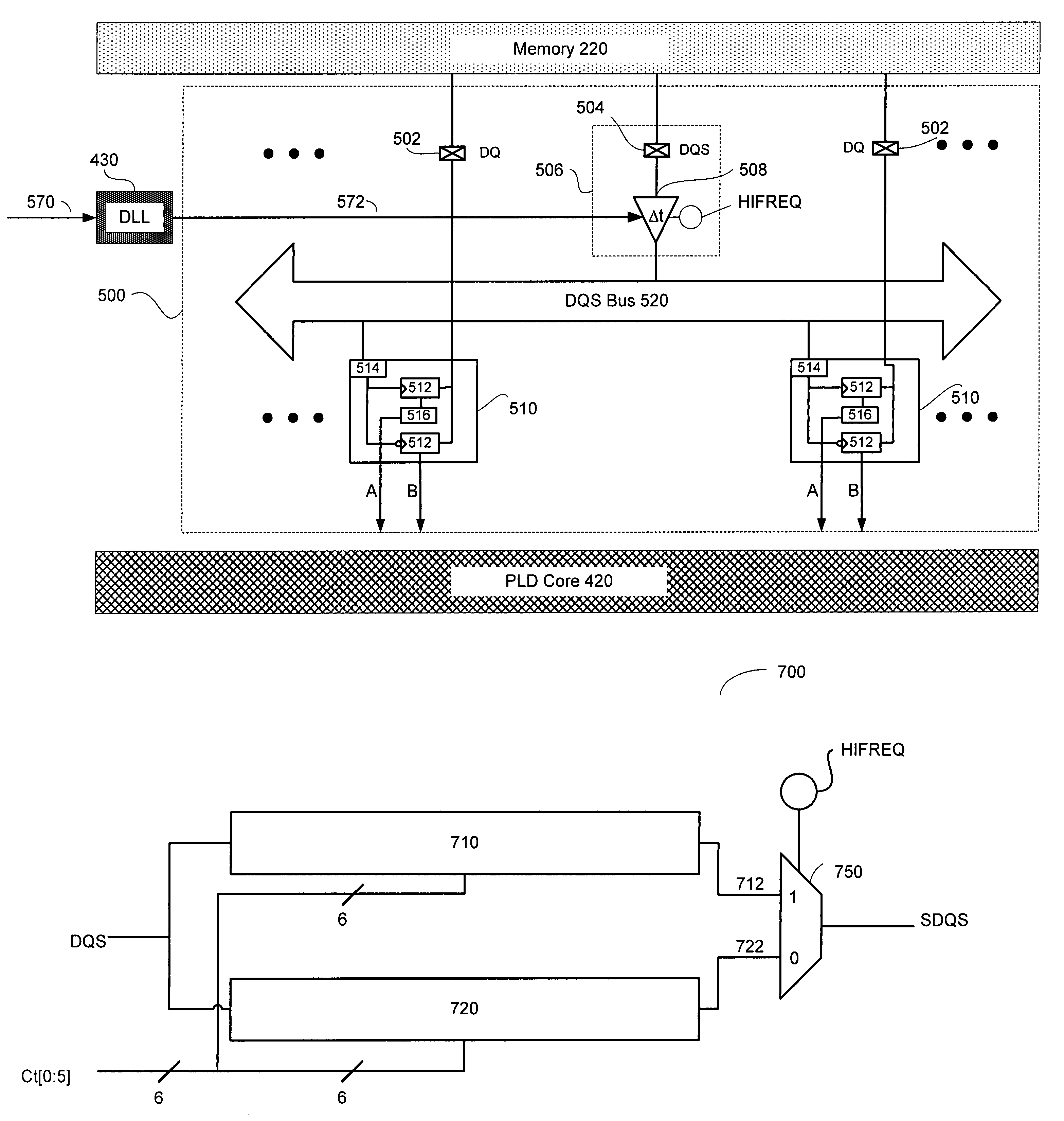
[0028]To support a wide range of memory frequencies, the present invention provides a phase-shift circuit that can be programmed to operate in one of multiple frequency ranges by using a different delay step and a different maximum delay for each of the multiple frequency ranges. For illustrative purposes, the invention is described in the context of a double-data rate (DDR) system. It is to be understood, however, that the principles of this invention can be applied to a variety of data rate systems.

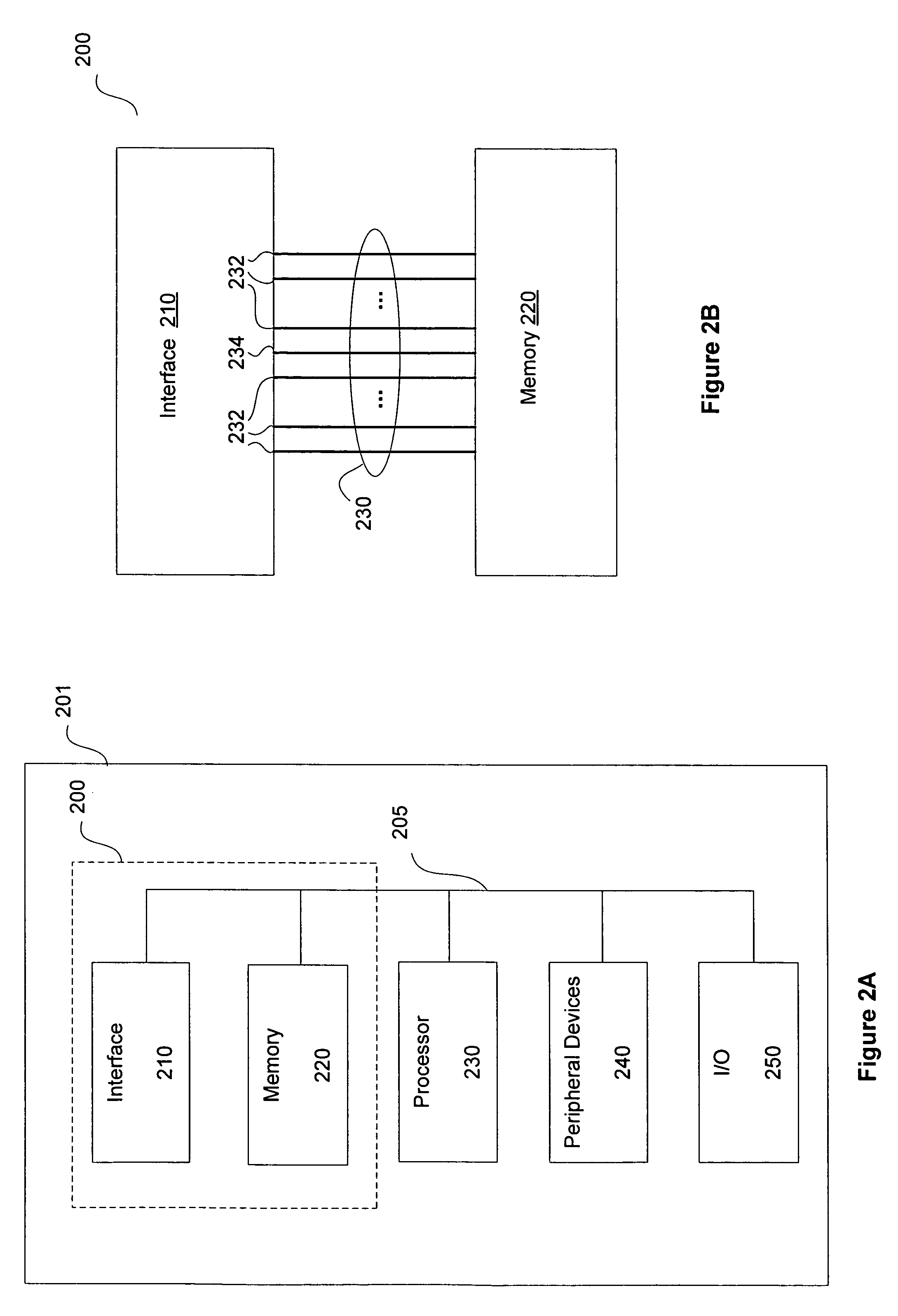
[0029]FIG. 2A is a block diagram of an exemplary system 200 including a memory interface circuit (interface) 210, and a multiple-data rate memory device 220, according to one embodiment of the present invention. System 200 may be part of a larger system 201, such as a data processing system, which may include one or more of the following components: a processor 230, peripheral devices 240, and input / output (I / O) device(s) 250, in addition to the components in system 200. The above compo...


PUM


Abstract

The present invention provides a phase shift circuit that supports multiple frequency ranges. The phase shift circuit receives a plurality of control bits and causes a phase shift in a received signal, the phase shift corresponding to a number of time steps, the number depending on the control bits, and the time step is selected from a plurality of different time steps based on a frequency range associated with the received signal.

Description

BACKGROUND OF THE INVENTION[0001]The present invention relates in general to input / output (I / O) interface architectures in integrated circuits, and in particular to memory interface phase-shift circuitry that supports multiple frequency ranges.[0002]Typical I / O architectures transmit a single data bit on each positive edge of a strobe signal and are limited to the speed of the strobe signal. To address the problem of data bandwidth bottleneck between integrated circuits, high speed interface mechanisms have been developed to increase the speed of data transfer and data throughput. In a multiple data rate (MDR) interface scheme, two or more data bits are transferred during each clock period of the strobe signal. For example, in a double data rate (DDR) interface scheme, data can be captured on both a rising edge and a falling edge of the clock to achieve twice the throughput of data. Multiple data rate technologies have thus accelerated the I / O performance of integrated circuits for ...

Claims


Application Information

Patent Timeline
Patent Type & Authority Patents(United States)
IPC IPC(8): H03H11/26
CPCG11C7/1006G11C7/22G11C7/222G11C11/4076G11C11/4096H03K2005/00058
Inventor LEE, ANDY L.
Owner BROOKE LAWRENCE L
Why Eureka
Try Eureka