Method and apparatus for determining transistor sizes

a transistor size and transistor technology, applied in the direction of cad circuit design, error detection/correction, instruments, etc., can solve the problem of the most difficult challenge for a designer

Active Publication Date: 2006-10-24
ORACLE INT CORP
View PDF4 Cites 98 Cited by
  • Summary
  • Abstract
  • Description
  • Claims
  • Application Information

AI Technical Summary

Benefits of technology

[0011]The method of logical effort analysis is described more completely in Logical Effort: Designing Fast CMOS Circuits, by Ivan Sutherland, Bob Sproull, and David Harris, Morgan Kaufman Publishers, Inc. (1999), ISBN # 1-55860-557-6.

Problems solved by technology

One of the most difficult challenges for a designer is laying out the circuit so that the circuit meets timing constraints.
Without a systematic approach, designers resort to continually simulating and modifying the design to achieve the timing constraints.

Method used


Image

  • Method and apparatus for determining transistor sizes
  • Method and apparatus for determining transistor sizes
  • Method and apparatus for determining transistor sizes

Examples


Embodiment Construction

[0021]The following description is presented to enable any person skilled in the art to make and use the invention, and is provided in the context of a particular application and its requirements. Various modifications to the disclosed embodiments will be readily apparent to those skilled in the art, and the general principles defined herein may be applied to other embodiments and applications without departing from the spirit and scope of the present invention. Thus, the present invention is not intended to be limited to the embodiments shown, but is to be accorded the widest scope consistent with the principles and features disclosed herein.

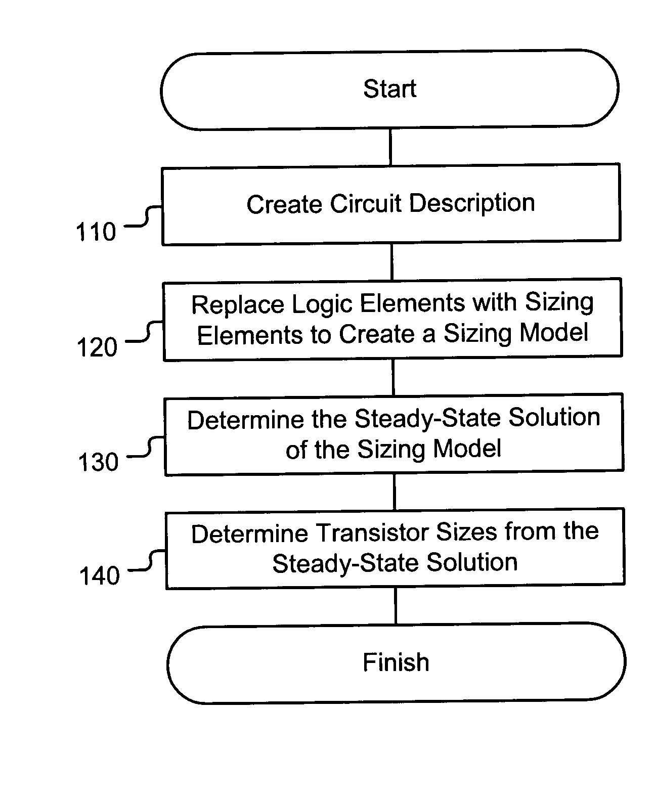
[0022]One embodiment of the invention is a method, shown in FIG. 1, that assists circuit designers in selecting logic gates from a library of logic gates.

5.1 Create a Circuit Description

[0023]The first step of the method shown in FIG. 1, which is shown in Block 110, is creating a circuit description. The circuit description details the various ...


PUM


Abstract

A method of determining at least one ratio of transistor sizes. The method includes creating a sizing model by replacing at least one logic element in a circuit description with a sizing element that includes a piece-wise-linear current source. The method also includes determining a steady state solution to the sizing mode and determining at least one ratio of transistor sizes from the steady state solution. The method may also include determining at least one dimension of a transistor based at least in part upon the ratio of transistor sizes.

Description

1. FIELD OF THE INVENTION[0001]The present invention generally relates to methods of designing integrated circuits. More specifically, the present invention relates to methods of designing integrated circuits that include performing a logical effort analysis that selects near optimal transistor gate widths from a predetermined group of transistor widths.2. BACKGROUND[0002]Integrated circuit (“IC”) design consists of a number of steps. Typically, the design starts with a specification of the functional performance characteristics of the IC. The IC is then typically broken down into more manageable blocks so that the blocks may be divided among multiple designers and analyzed in pieces by computer aided design tools. Next, logic designers write register transfer level (“RTL”) descriptions of each block. Next, floor plans are created for each of the blocks. After verifying that the RTL descriptions are accurate, the designers estimate the size of each block. Then designers create a flo...

Claims


Application Information

Patent Timeline
Patent Type & Authority Patents(United States)
IPC IPC(8): G06F17/50
CPCG06F17/5031G06F17/5045G06F30/3312G06F30/30
Inventor SIGNORE, NICHOLAS D.
Owner ORACLE INT CORP
Why Eureka
Try Eureka