Method of making a three-dimensional stacked semiconductor package with a metal pillar in an encapsulant aperture
Inactive Publication Date: 2006-10-31
BRIDGE SEMICON
View PDF176 Cites 32 Cited by
Summary
Abstract
Description
Claims
Application Information
AI Technical Summary
This helps you quickly interpret patents by identifying the three key elements:
Problems solved by technology
Method used
Benefits of technology
Benefits of technology
[0075]An advantage of the present invention is that the three-dimensional package can be manufactured conveniently and cost effectively. Another advantage is that the package can contain ultra-thin, first-level, single-chip assemblies in an integrated module, and can be directly mounted on a printed circuit board. Another advantage is that the package can accommodate chips with varying sizes and thickness while maintaining reliable pillar connections. Another advantage is that the package is well-suited for testing, disassembly and reworking. Another advantage is that the metal particles can be pre-made rather than deposited on the routing lines by electroplating or electroless plating which improves uniformity and reduces manufacturing time and cost. Another advantage is that the connection joints can be made from a wide variety of materials and processes, thereby making advantageous use of mature connect
Problems solved by technology
However, significant obstacles to further reduction in feature size are being encountered.
These obstacles include defect density control, optical system resolution limits, and availability of processing material and equipment.
In addition, flip-chip bonding requires minimal mounting area and weight which results in overall cost saving since no extra packaging and less circuit board space are used.
While flip-chip technology has tremendous advantages over wire bonding and TAB, its cost and technical limitations are significant.
For instance, the cost of forming bumps on the pads is significant.
In addition, an adhesive is normally underfilled between the chip and the support circuit to reduce stress on the solder joints due to thermal mismatch between the chip and the support circuit, and the underfilling process increases both manufacturing complexity and cost.
Thus, none of these conventional connection techniques are entirely satisfactory.
Conventional single-chip packages typically have an area (or footprint) that is many times larger than the area of the chip, causing the printed circuit board to have excessively large area relative to the chips.
However, as chip speeds increase, it becomes critical to position the chips close together since excessive signal transmission distance deteriorates signal integrity and propagation times. Other considerations such as manufacturing cost, reliability, heat transfer, moisture resistance, mounting and interconnect standardization, testability, and quality control have also become focal points of chip packaging.
Although these packages provide certain advantages, further size reduction and performance enhancement with these packages has been difficult to obtain due to physic
Method used
Image
Click on the blue label to locate the original text in one second.
Reading with bidirectional positioning of images and text.
Examples
Example
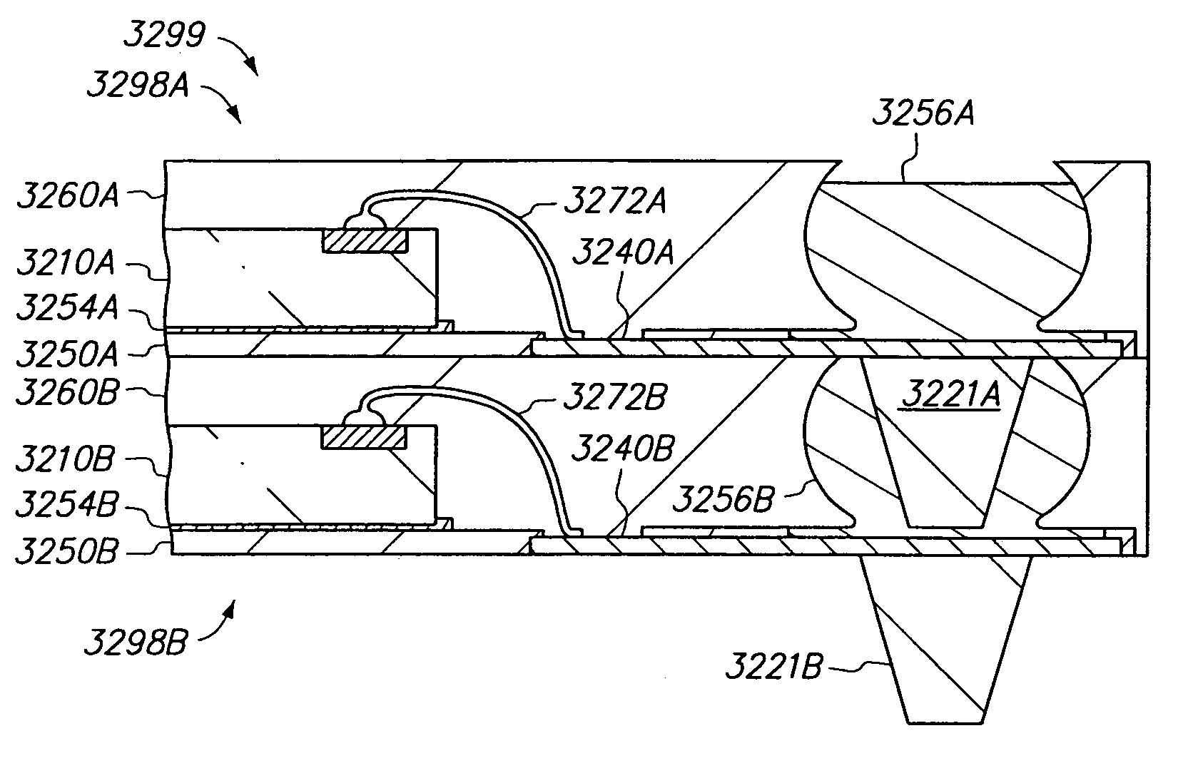
[0278]The grinding is applied longer than in the first embodiment and removes portions of chip 1010, metal particle 1056 and encapsulant 1060. Initially, the diamond sand wheel grinds only encapsulant 1060. As the grinding continues, encapsulant 1060 becomes thinner as its grinded surface migrates downwardly. Eventually the diamond sand wheel contacts metal particle 1056, and as a result, begins to grind metal particle 1056 as well. As the grinding continues, metal particle 1056 and encapsulant 1060 become thinner as their grinded surfaces migrate downwardly. However, the grinding does not halt before it reaches chip 1010. Instead, the grinding continues and eventually the diamond sand wheel contacts chip 1010, and as a result, begins to grind chip 1010 as well. As the grinding continues, chip 1010, metal particle 1056 and encapsulant 1060 become thinner as their grinded surfaces migrate downwardly. The grinding continues until chip 1010, metal particle 1056 and encapsulant 1060 hav...
PUM
Abstract
A method of making a three-dimensional stacked semiconductor package includes providing a first semiconductor chip assembly that includes a first chip, a first conductive trace and a first encapsulant, wherein the first conductive trace includes a first metal pillar, providing a second semiconductor chip assembly that includes a second chip, a second conductive trace and a second encapsulant, wherein the second encapsulant includes a second aperture, and then positioning the first and second assemblies such that the first assembly overlaps the second assembly and the first metal pillar extends into the second aperture.
Description
CROSS-REFERENCE TO RELATED APPLICATIONS[0001]This application is a continuation of U.S. application Ser. No. 10 / 966,816 filed Oct. 15, 2004, now U.S. Pat. No. 7,067,911, which is a continuation-in-part of U.S. application Ser. No. 10 / 922,280 filed Aug. 19, 2004, now U.S. Pat. No. 7,009,297, which is a continuation-in-part of U.S. application Ser. No. 10 / 307,218 filed Nov. 29, 2002, now U.S. Pat. No. 6,809,414, which is a divisional of U.S. application Ser. No. 09 / 997,973 filed Nov. 29, 2001, now U.S. Pat. No. 6,492,252, which is a continuation-in-part of U.S. application Ser. No. 09 / 917,339 filed Jul. 27, 2001, now U.S. Pat. No. 6,537,851, which is a continuation-in-part of U.S. application Ser. No. 09 / 878,626 filed Jun. 11, 2001, now U.S. Pat. No. 6,653,217, which is a continuation-in-part of U.S. application Ser. No. 09 / 687,619 filed Oct. 13, 2000, now U.S. Pat. No. 6,440,835, each of which is incorporated by reference.[0002]U.S. application Ser. No. 10 / 922,280 filed Aug. 19, 2004...
Claims
Application Information
Patent Timeline
Application Date:The date an application was filed.
Publication Date:The date a patent or application was officially published.
First Publication Date:The earliest publication date of a patent with the same application number.
Issue Date:Publication date of the patent grant document.
PCT Entry Date:The Entry date of PCT National Phase.
Estimated Expiry Date:The statutory expiry date of a patent right according to the Patent Law, and it is the longest term of protection that the patent right can achieve without the termination of the patent right due to other reasons(Term extension factor has been taken into account ).
Invalid Date:Actual expiry date is based on effective date or publication date of legal transaction data of invalid patent.

