Liquid crystal display panel and liquid crystal display thereof

a liquid crystal display and panel technology, applied in the field of liquid crystal display panel and liquid crystal display thereof, can solve the problems of user's inability to see an image displayed at a certain time overlapped, image quality deterioration, and rc delay in the transmission of scanning signals, so as to increase the charging time of a display datum and high resolution

Active Publication Date: 2006-10-31
HANNSTAR DISPLAY CORPORATION
View PDF9 Cites 12 Cited by
  • Summary
  • Abstract
  • Description
  • Claims
  • Application Information

AI Technical Summary

Benefits of technology

[0010]The first object of the present invention is to increase the charging time of a display datum on the LCD with a high resolution by adding a TFT in each pixel to enable a black voltage to be written in the corresponding LC capacitor.

Problems solved by technology

However, for the dynamic image which displays a continuous movement, the image quality deteriorates due to a residual image phenomenon.
Therefore, a user can never see an image displayed at a certain time overlapped with a previous image.
In fact, the RC delay arises in the transmission of the scanning signal, which is especially relevant to the LCD with a large size or high resolution.
In other words, the existence of the gate delay will shorten the actually working time of a display datum, and TFT is delayed to completely turn itself off.
In conclusion, the prior art limits the charging time of the LC capacitor to the critically write-in time of a display datum 181, so the image quality deteriorates due to this limitation.
Such an insufficient charging time is the bottleneck of upgrading the size and resolution of an LCD.

Method used


Image

  • Liquid crystal display panel and liquid crystal display thereof
  • Liquid crystal display panel and liquid crystal display thereof
  • Liquid crystal display panel and liquid crystal display thereof

Examples


Embodiment Construction

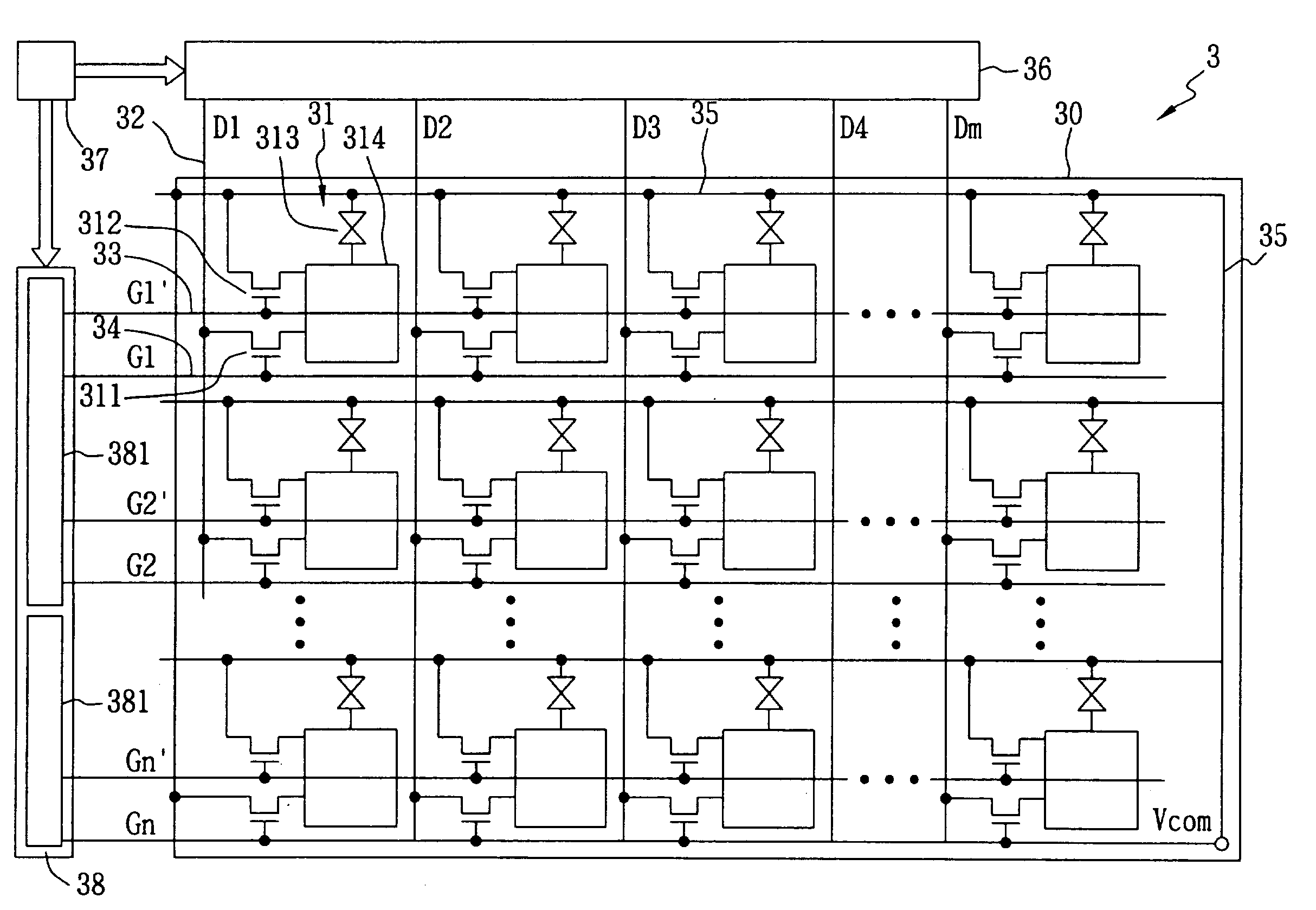
[0022]Please refer to FIG. 3, which shows the configuration of an LCD 3 in accordance with the embodiment of the present invention. The scanning lines, G1–Gn 34, are formed on a transparent insulating substrate such as a glass substrate in a transverse direction. The black selecting lines, G1′–Gn′33, which are accompanied with the scanning lines, G1–Gn 34, in parallel, goes across each row of pixels on the LCD panel 30.

[0023]A first switching element formed in the pixel 31 is named as a first TFT 311 whose gate terminal is connected to the scanning line, G1311, and two other terminals are respectively connected to a pixel electrode 314 and the signal line, D132. A second switching element also formed in the pixel 31, is named as a second TFT 312 whose gate terminal is connected to the black selecting line, G1′33, and the other two terminals are respectively connected to the pixel electrode 314 and a common electrode 35. The electrical field in the LC capacitor 313, whose two termina...


PUM

PropertyMeasurementUnit
gradation voltageaaaaaaaaaa
voltageaaaaaaaaaa
timeaaaaaaaaaa

Abstract

A liquid crystal display has a plurality of pixels arranged in a matrix to be formed on a transparent insulating substrate. A first switching element formed in each pixel is a three-terminal TFT whose gate terminal is connected to the scanning line and two other terminals are respectively connected to a pixel electrode and a signal line. Furthermore, a second switching element formed in each pixel is a three-terminal TFT whose gate terminal is connected to a black selecting line and two other terminals are respectively connected to the pixel electrode and a common electrode.

Description

BACKGROUND OF THE INVENTION[0001]1. Field of the Invention[0002]The present invention relates to a liquid crystal display (LCD) panel and a liquid crystal display thereof, and more particularly to an active matrix LCD suitable for displaying a dynamic image.[0003]2. Description of the Related Art[0004]The manufacturing technique for LCDs has progressed in the manufacture of high contrast displays with a wide view angle. However, for the dynamic image which displays a continuous movement, the image quality deteriorates due to a residual image phenomenon. Recently, there have been many relative driving methods to improve the image quality of LCDs, and the black data insertion method provided by NEC Corporation is one suitable solution upon the dynamic image issue. The prior art applies the voltage of a black datum in a sequence to the Liquid crystal (LC) capacitor of each pixel during a frame period so as to have an “impulse-type” effect on the same display as a cathode ray tube (CRT)...

Claims


Application Information

Patent Timeline
Patent Type & Authority Patents(United States)
IPC IPC(8): G09G3/36G02F1/1368G02F1/133G09F9/30G09F9/35G09G3/20
CPCG09G3/3659G09G3/2011G09G2300/043G09G2320/0261G09G2310/0289G09G2310/061G09G2300/0814
Inventor SHIN, SEOB
Owner HANNSTAR DISPLAY CORPORATION
Why Eureka
Try Eureka