Fully programmable phase locked loop

a phase lock loop, fully programmable technology, applied in the field of electronic devices, can solve the problems of reducing the size of electronic devices, not being able to scale well, and not being able to meet the needs of newer process technologies

Active Publication Date: 2006-11-14
APPLE INC
View PDF6 Cites 20 Cited by
  • Summary
  • Abstract
  • Description
  • Claims
  • Application Information

AI Technical Summary

Problems solved by technology

The conventional PLL architecture is not ideal for newer process technologies, does not scale well from one process technology to the next, and must be redesigned for use in various electronic devices in different markets.
The drive to reduce the size of electronic devices has increased the difficulty of implementing capacitors in a semiconductor device.
In particular, reducing the thickness of gate oxides increases the gate leakage currents of semiconductor capacitor devices.
Reducing the thickness of the insulator, however, increases the leakage currents of the semiconductor capacitor devices.
The transistors implemented using advanced CMOS processes, such as 90-nm (nanometer) CMOS, are exhibiting non-ideal behavioral traits for implementation of critical analog functions, such as current and voltage sources or references, VCO's, charge pumps, etc.
Some of these non-ideal transistor traits include increased gate tunneling current, increased drain-source leakage, reduced voltage headroom due to VDD scaling, and increased noise susceptibility due to decreased threshold voltages.
Furthermore, with respect to PLL design, the very high gain VCOs are causing increased cycle-to-cycle jitter, coupled with increased phase drift due to the ever increasing discrepancy between the internal speed of the processor and the interface reference clock speeds.
Fully digital PLLs can alleviate some of the issues but do not scale very well.
Furthermore, the need to integrate more PLLs on chip for System-On-Chip (SOC) applications forces more unique PLL implementations which cause design overhead and risk.
The clocks oscillate at different voltage levels and with different slopes on the rising and falling edges, and thus are difficult to match for de-skew control.
Dual-Gate Oxide (DGO) or “thick-gate” transistors are used to withstand the higher voltage levels, but do not operate well at the lower voltage levels.
Single-Gate Oxide (SGO) or “thin-gate” transistors are smaller and faster and optimized for low voltage operation, but are unable to handle the higher voltage levels.
Also, such interface to higher voltage devices was a less than optimal solution that complicated skew control and that was difficult to optimize when the PLL was required to operate over a wide range of supply voltage.

Method used


Image

  • Fully programmable phase locked loop
  • Fully programmable phase locked loop
  • Fully programmable phase locked loop

Examples


Embodiment Construction

[0019]The following description is presented to enable one of ordinary skill in the art to make and use the present invention as provided within the context of a particular application and its requirements. Various modifications to the preferred embodiment will, however, be apparent to one skilled in the art, and the general principles defined herein may be applied to other embodiments. Therefore, the present invention is not intended to be limited to the particular embodiments shown and described herein, but is to be accorded the widest scope consistent with the principles and novel features herein disclosed.

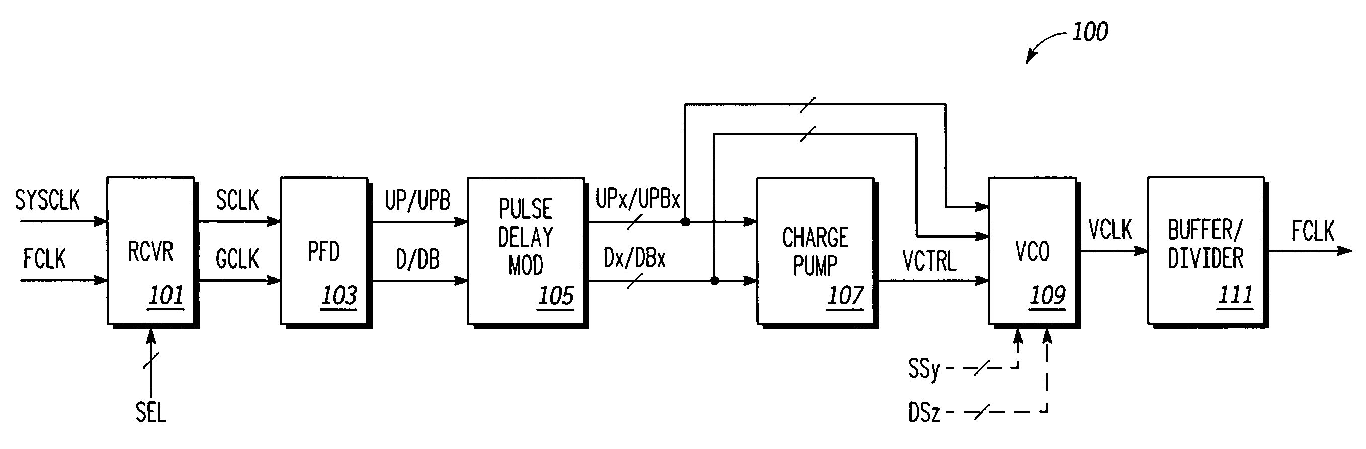
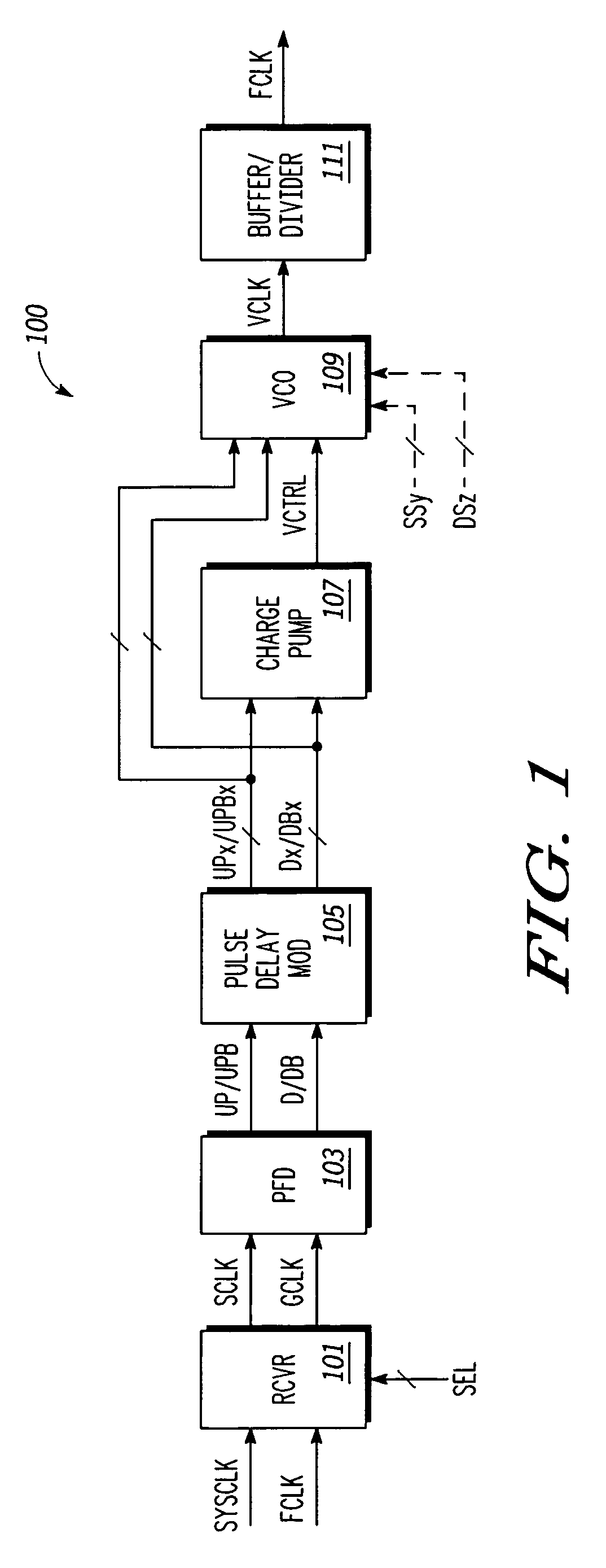
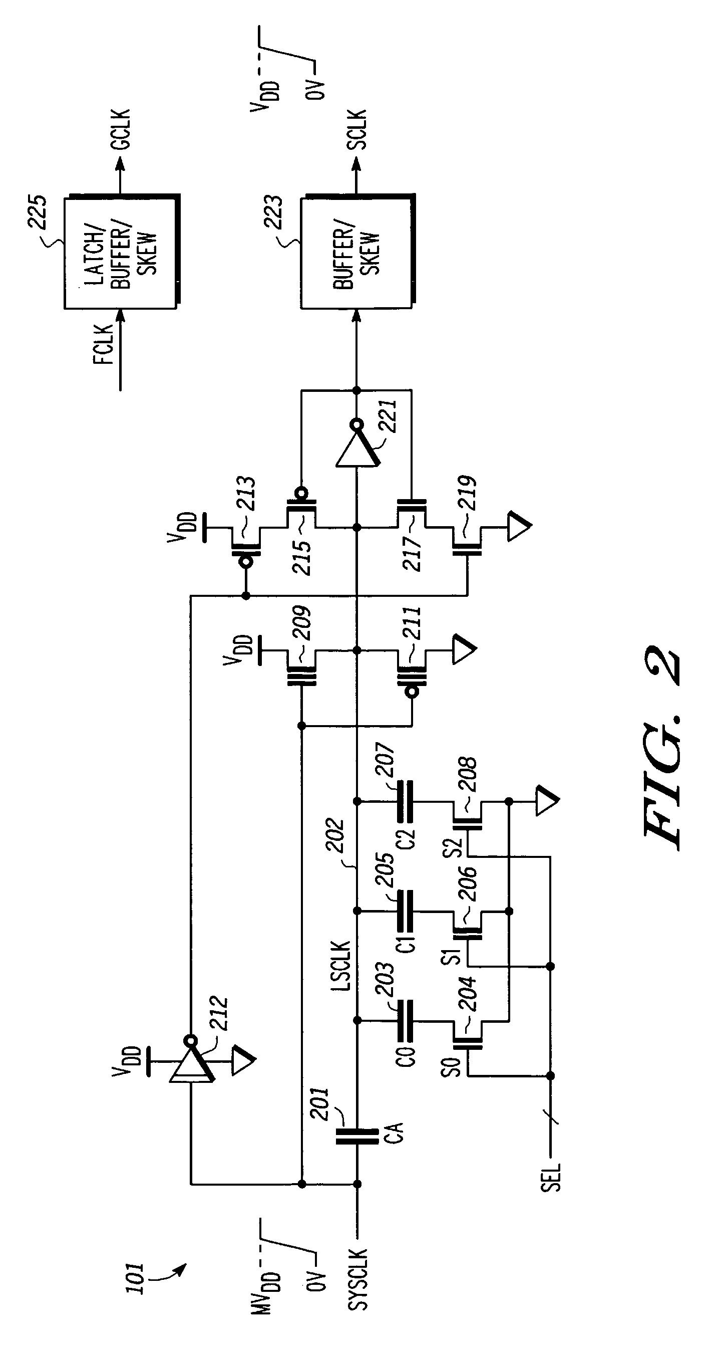
[0020]FIG. 1 is a block diagram of a phase locked loop (PLL) 100 implemented according to an exemplary embodiment of the present invention. The PLL 100 includes an output for providing an output clock signal (FCLK) that may be at the same frequency, a fractional frequency, or multiple frequency of a reference or system clock signal referred to as SYSCLK. The SYSCLK and FCLK sig...


PUM


Abstract

A programmable PLL including a receiver, a phase frequency detector, a charge pump, and a VCO. The receiver includes a programmable capacitor voltage divider that shifts voltage of an input clock to provide a level-shifted clock. The AC interface includes a state detection and correction circuit that ensures proper state of the level-shifted clock. The PLL includes a pulse delay modulator for generating delayed clock control signals. The VCO includes a programmable phase control circuit that dynamically adjusts phase using the delayed clock control signals. The VCO circuit includes a ring oscillator circuit with one or more phase control nodes. The programmable phase control circuit selectively couples devices to the phase control node using the clock control signals to adjust phase. The devices may be capacitors or transistors, each switched using switches controlled by the delayed clock control signals. The capacitors may be metal capacitors or semiconductor transistor capacitors.

Description

BACKGROUND OF THE INVENTION[0001]1. Field of the Invention[0002]The present invention relates in general to electronic devices and specifically to a fully programmable phase locked loop.[0003]2. Description of the Related Art[0004]Phase locked loops (PLLs) are utilized by electronic devices to generate clock signals from a reference signal. The generated clock signal maybe at the same frequency as the reference clock signal or at a fractional or multiple frequency of the reference clock signal. The generated clock signal typically has a predetermined phase relationship with the reference clock signal.[0005]A typical PLL includes a phase frequency detector (PFD), a charge pump, and a voltage controlled oscillator (VCO), among other supporting circuitry. The PFD compares an input or system clock with an output clock and provides clock control signals to the charge pump. The charge pump adds or subtracts charge to a filter capacitor based on the clock control signals and generates a co...

Claims


Application Information

Patent Timeline
Patent Type & Authority Patents(United States)
IPC IPC(8): H03L7/089H03L7/099
CPCH03K3/0377H03K5/084H03K5/133H03L7/0896H03L7/0995H03K2005/00071
Inventor SANCHEZ, HECTORGREAVES, CARLOS A.NISSEN, JIM P.TANG, XINGHAI
Owner APPLE INC
Why Eureka
Try Eureka