Frequency selective high impedance surface

a high-impedance surface, frequency selective technology, applied in the direction of radiating element structure forms, resonance antennas, antenna earthings, etc., can solve the problem of excessively large high-impedance surfaces that must be used

Active Publication Date: 2006-11-14
NXP USA INC
View PDF13 Cites 53 Cited by
  • Summary
  • Abstract
  • Description
  • Claims
  • Application Information

AI Technical Summary

Problems solved by technology

Upon reaching an edge, corner or other discontinuity, these surface waves radiate, or scatter, resulting in interference.
The presence of such interference, therefore, is a cause for concern for high-frequency device designers using conductive materials, such as, for example, ground planes or reflectors for antennas, microstrip transmission lines, inductors, and the like.
However, to achieve the inductance and capacitance necessary for a number of desirable operating frequency ranges, excessively large high-impedance surfaces often must be used due to the limited inductance and capacitance supplied by conventional conductive structures.

Method used


Image

  • Frequency selective high impedance surface
  • Frequency selective high impedance surface
  • Frequency selective high impedance surface

Examples


Embodiment Construction

[0023]The following description is intended to convey a thorough understanding of specific embodiments and details involving high-impedance surfaces. It is understood, however, that the present disclosure is not limited to these specific embodiments and details, which are exemplary only. It is further understood that one possessing ordinary skill in the art, in light of known systems and methods, would appreciate the use of the invention for its intended purposes and benefits in any number of alternative embodiments, depending upon specific design and other needs.

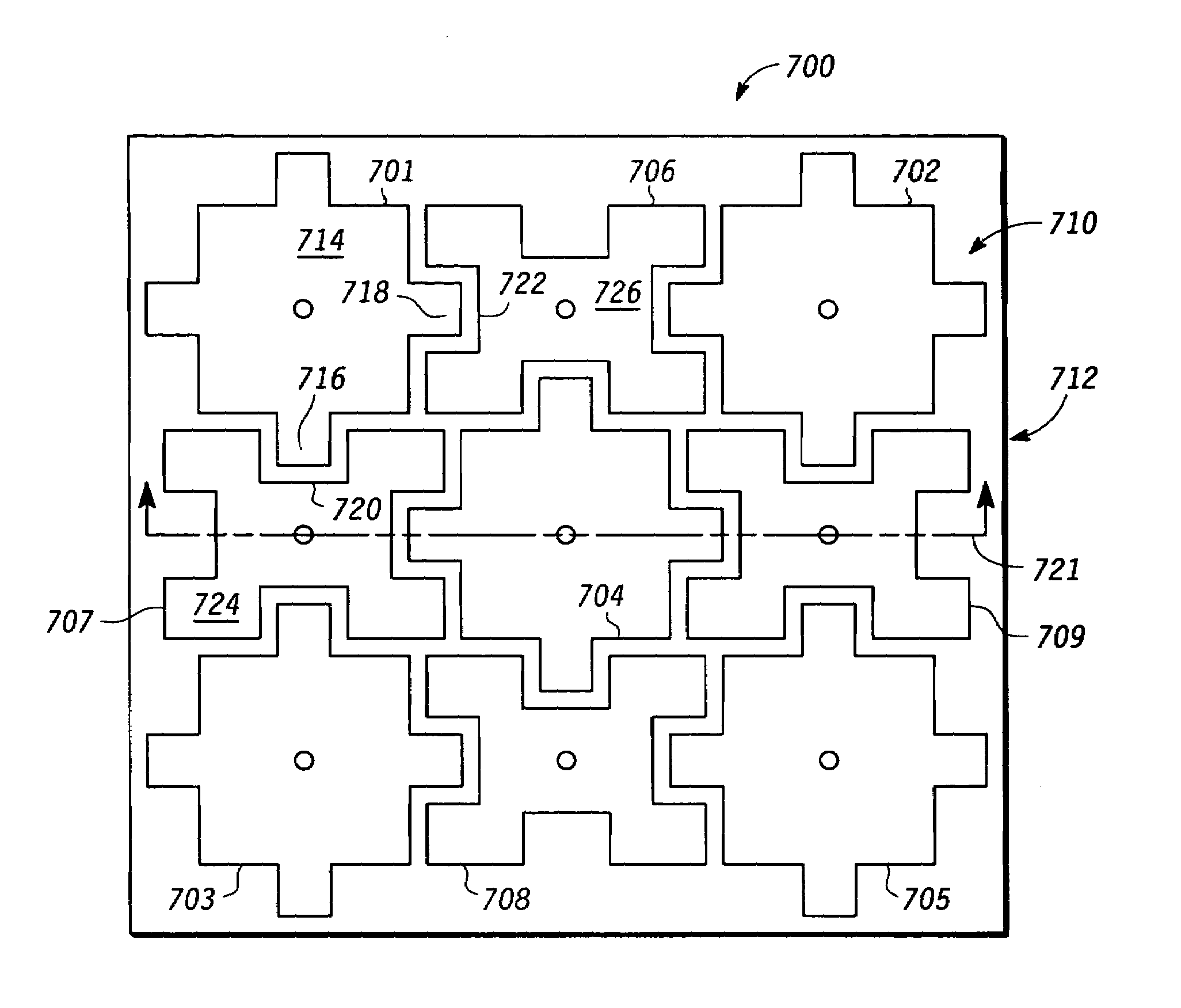
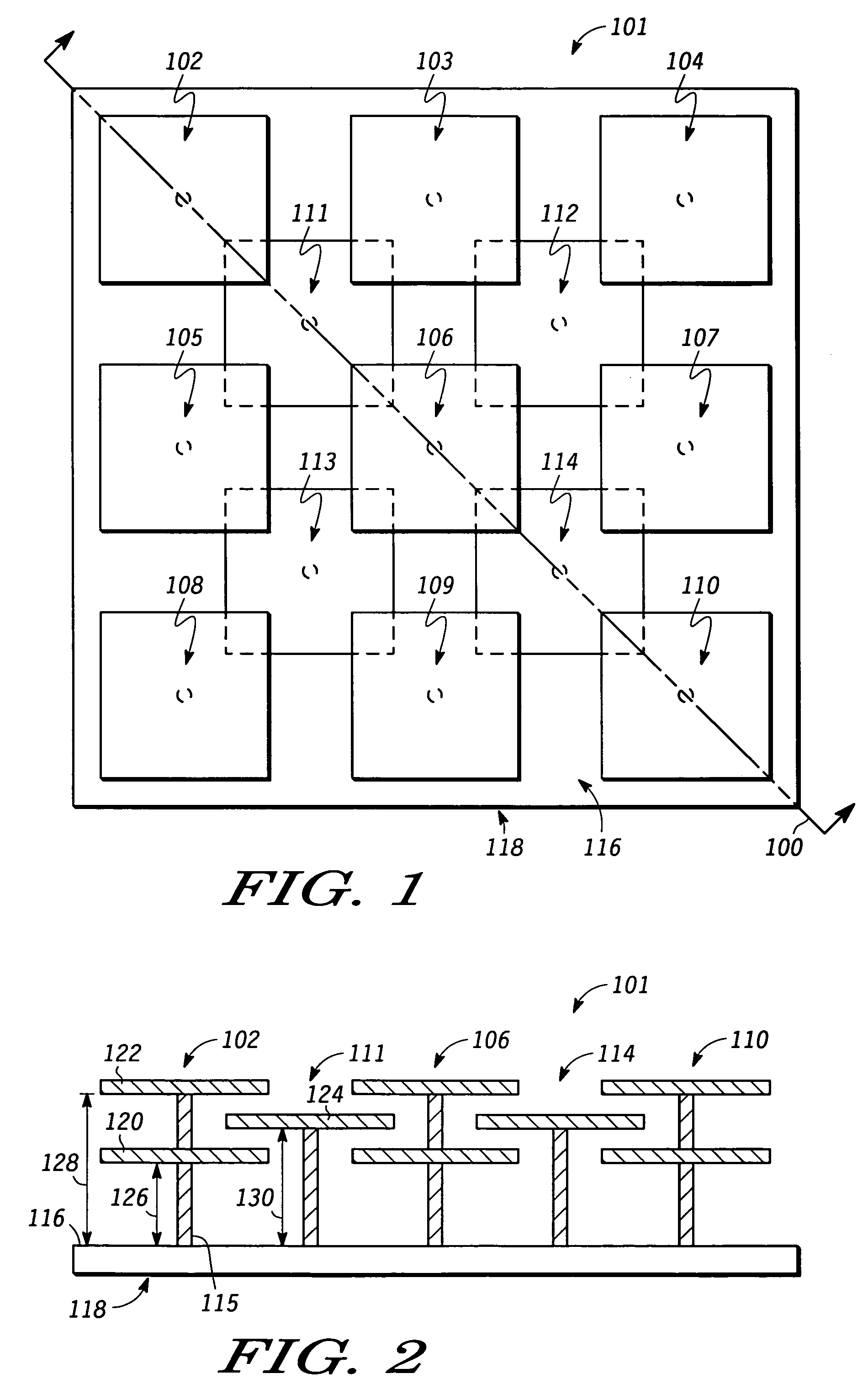
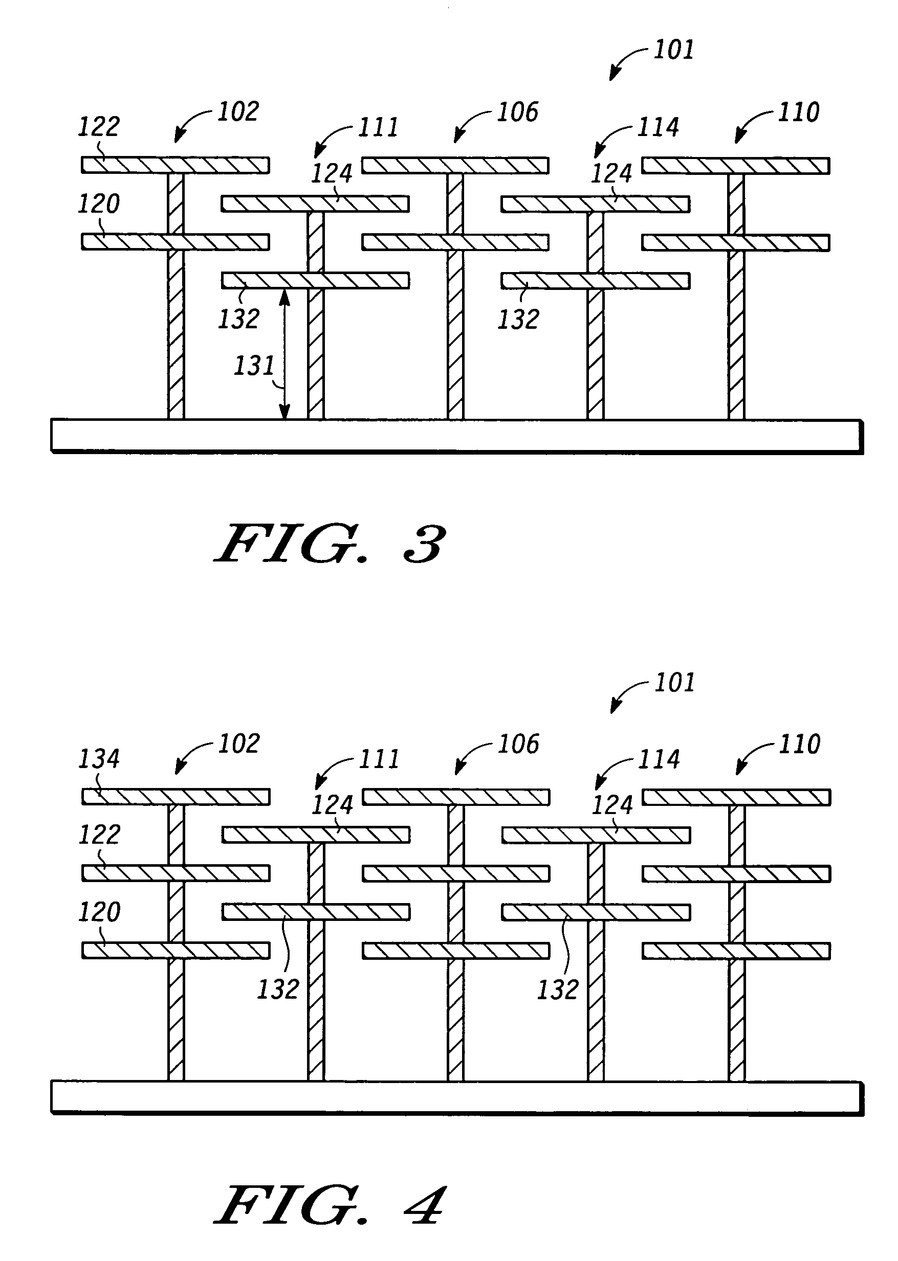
[0024]FIGS. 1–35 illustrate high-impedance surfaces and techniques for their implementation. In at least one embodiment, a high-impedance surface incorporates a lattice of conductive structures having two or more conductive plates substantially in parallel, where the conductive plates are interleaved with the conductive plates of one or more adjacent conductive structures in the lattice. In another embodiment, the perimeter...


PUM


Abstract

Disclosed herein are various high-impedance surfaces having high capacitance and inductance properties. One exemplary high-impedance surface includes a plurality of conductive structures arranged in a lattice, wherein at least a subset of the conductive structures include a plurality of conductive plates arranged along a conductive post so that the conductive plates of one conductive structure interleave with one or more conductive plates of one or more adjacent conductive structure. Another exemplary high-impedance surface includes a plurality of conductive structures arranged in a lattice, where the conductive structures include one or more fractalized conductive plates having either indentions and / or projections that are coextensive with corresponding projections or indentations, respectively, of one or more adjacent conductive structures. Also disclosed are various exemplary implementations of such high-impedance surfaces.

Description

CROSS-REFERENCE TO RELATED APPLICATIONS[0001]The present application is related to co-pending U.S. patent application Ser. No. 10 / 927,921, filed herewith and entitled “Applications of a High Impedance Surface”, the entirety of which is incorporated by reference herein.FIELD OF THE INVENTION[0002]The present disclosure relates generally to high-impedance surfaces and more particularly to frequency tunable high-impedance surfaces.BACKGROUND OF THE INVENTION[0003]A smooth-surfaced conductor typically has low surface impedance, which results in the propagation of electromagnetic (EM) waves at the surface of the conductor at higher frequencies. Upon reaching an edge, corner or other discontinuity, these surface waves radiate, or scatter, resulting in interference. The presence of such interference, therefore, is a cause for concern for high-frequency device designers using conductive materials, such as, for example, ground planes or reflectors for antennas, microstrip transmission lines,...

Claims


Application Information

Patent Timeline
Patent Type & Authority Patents(United States)
IPC IPC(8): H01Q15/02H01Q1/38
CPCH01Q1/22H01Q1/48H01Q15/008
Inventor RAMPRASAD, RAMAMURTHYPETRAS, MICHAEL F.TSAI, CHI TAOU
Owner NXP USA INC
Why Eureka
Try Eureka