

Plasma display device having improved luminous efficacy
- Summary
- Abstract
- Description
- Claims
- Application Information
AI Technical Summary
Benefits of technology
Problems solved by technology
Method used
Image

Examples
example 1 of embodiment 1
OF THE PRESENT INVENTION
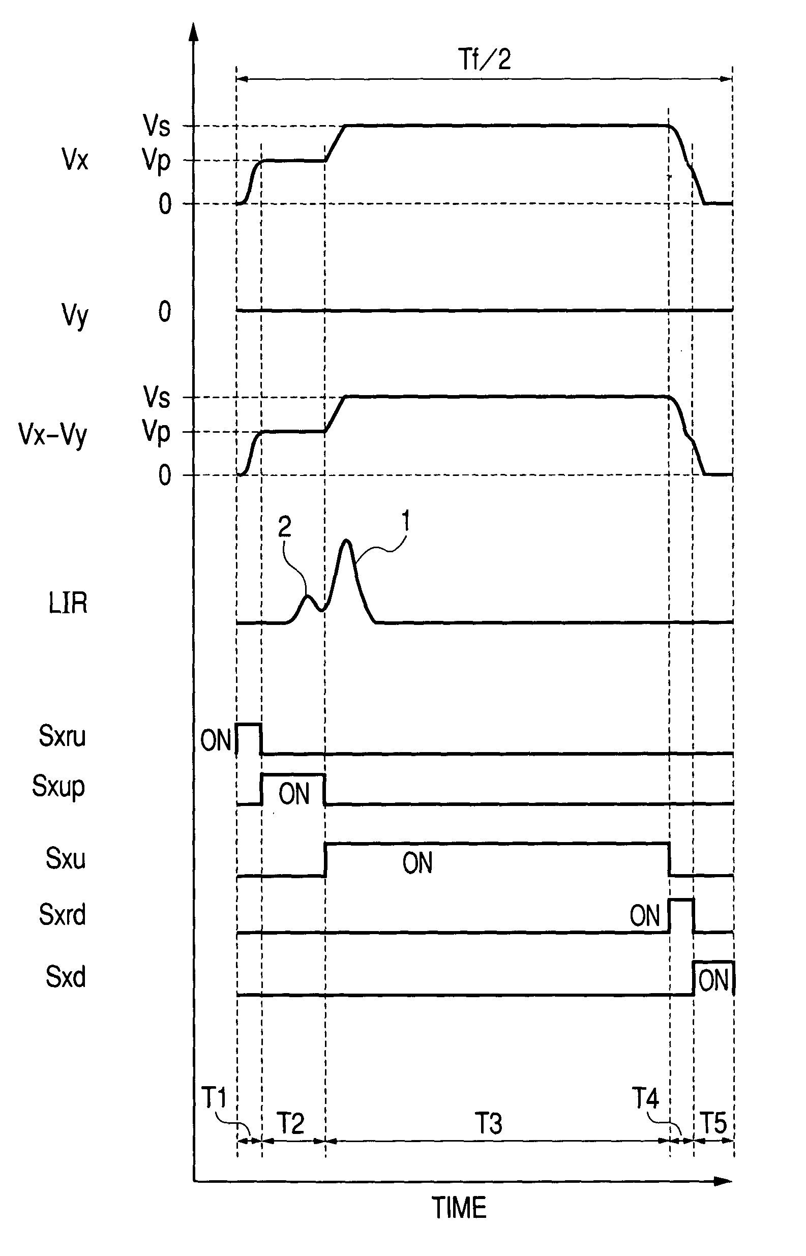
[0087]FIG. 3 is a diagram of the X electrode driving circuit 95a of the plasma display device 100a of Example 1 of Embodiment 1 in accordance with the present invention, for explaining its operation during the sustain period. For simplicity, the same symbols (Sxru-Sxd) as utilized to denote the input signals to the switches in FIG. 1 designate the corresponding switches (formed by transistors in practice) in FIG. 3. The same shall apply hereinafter.
[0088]The X electrode driving circuit 95a comprises a power recover circuit 101 composed of switches Sxru, Sxrd, diodes Dxru, Dxrd, a power recovery capacitor Cxr, a power recovery coil Lxr, and a grounding terminal GND; switches Sxu, Sxd, Sxup; power supplies for supplying voltages Vs, Vp; and a grounding terminal GND. Although the Y electrode driving circuit 96a is not shown in FIG. 3, it is similar to the X electrode driving circuit 95a, and its circuit components are denoted by symbols with the suffix y in plac...
example 2 of embodiment 1
OF THE PRESENT INVENTION
[0121]In the above Example 1 of the Embodiment 1, the intermediate voltage Vp is provided by using a power supply. In the following, Example 2 of Embodiment 1 will be explained which employs an inductance Lp for production of the intermediate voltage Vp.
[0122]FIG. 4 is a time chart illustrating sustain pulse waveforms Vx, Vy applied to all the X and Y electrodes, respectively, simultaneously, a light emission waveform LIR, and input signals Sxru-Sxrd to switches of an X electrode driving circuit 95b shown in FIG. 5 during the sustain period 81 (see FIG. 18A) in a plasma display device of Example 2 of Embodiment 1 in accordance with the present invention. The X electrode driving circuit 95b of FIG. 5 differs from the X electrode driving circuit 95a of FIG. 3, in that the power supply for the voltage VP of the switch Sxup of FIG. 3 are not present in FIG. 5, and in that an inductance element Lxp such as a coil is provided between the switch Sxd and the ground G...
example 3 of embodiment 1
OF THE PRESENT INVENTION
[0126]In Example 3 of Embodiment 1 of the present invention, as a means for accumulating many wall charges when the load factor is increased, a voltage (hereinafter a post-discharge voltage) is applied around a time when a main discharge by one sustain pulse ceases such that an absolute value of a voltage difference Vs−Vy, a voltage between the sustain electrode pair, exceeds the voltage Vs.
[0127]As shown in FIG. 6, basically, if a voltage (−Vpp) is superimposed upon the sustain pulse Vy of FIG. 1 for Example 1 of Embodiment 1 after cessation of the main discharge 1, for example, the voltage difference Vx−Vy becomes Vs+Vpp. The voltage Vpp can be selected to be 20 V, for example.
[0128]Usually, when the main discharge has ceased, the wall charges of the polarities opposite to those of the respective electrodes are accumulated, and the discharge-space voltage is low, but space charges such as ions, electrons, and metastable particles are present, and are conver...
PUM
 Abstract
Description
Claims
Application Information