Method of manufacturing semiconductor device

a manufacturing method and semiconductor technology, applied in semiconductor devices, capacitors, electrical devices, etc., can solve the problems of deterioration of the remanent polarization characteristic relative high voltage required, and deterioration of the ferroelectric capacitor, so as to achieve excellent and uniform maintenance

Inactive Publication Date: 2006-12-26
FUJITSU SEMICON LTD
View PDF14 Cites 6 Cited by
  • Summary
  • Abstract
  • Description
  • Claims
  • Application Information

AI Technical Summary

Benefits of technology

[0015]It is an object of the present invention to provide a method of manufacturing a semiconductor device where the characteristics of capacitors covered by an interlayer insulating film can be maintained excellently and uniformly, or can be improved.
[0017]According to the present invention, the stress-controlling insulating film is deposited on the rear surface of the substrate after formation of the second insulating film coating the capacitor. For example, the stress-controlling insulating film is formed so as to have the same compressive stress or the same tensile stress as the second insulating film. Thus, the stress generated by the second insulating film is loosened and uniform stress adjustment can be performed. As a result, the characteristics of the capacitors can be maintained excellently and uniformly or the characteristics can be improved. According to an experiment by the inventors of the present invention, the characteristics and their variation could be improved when the present invention was applied to the method of manufacturing an FeRAM provided with a capacitor insulating film of ferroelectric.
[0018]Further, since the stress can be reduced on the entire wafer, so-called edge deterioration that occurs remarkably on the FeRAM of a planar structure can be prevented. The edge deterioration is a phenomenon that stress concentrates on the side portion of the dielectric film of the capacitors, which is at an edge portion of a lower electrode common to the plurality of capacitors, and thus the capacitor characteristics are inclined to deteriorate. The phenomenon could occur when an insulating film, which is formed by using TEOS as a material, is formed on the capacitors.

Problems solved by technology

Tunnel current passing through a gate insulating film needs to be flown in order to write and erase information, and thus relatively high voltage is required.
Meanwhile, when the first wiring pattern is formed of aluminum, the remanent polarization characteristic of the ferroelectric capacitor deteriorates due to the tensile stress of the first wiring pattern.
Therefore, when a plurality of interlayer insulating films are formed on the ferroelectric capacitors in a laminated manner, contractive force is applied to the ferroelectric capacitors every film forming step, and thus it deteriorates the ferroelectric capacitors.
Further, according to Document 2, since the interlayer insulating film still exists in spaces between the first wiring patterns, there is still a problem that the compressive stress of the interlayer insulating film deteriorates the ferroelectric capacitors regardless of the stress of the first wiring pattern.
Furthermore, according to Document 3, the interlayer insulating film having tensile stress has high moisture content, and thus it results in another problem such that the moisture deteriorates the ferroelectric capacitors.

Method used


Image

  • Method of manufacturing semiconductor device
  • Method of manufacturing semiconductor device
  • Method of manufacturing semiconductor device

Examples


Embodiment Construction

[0034]The embodiments of the present invention will be explained as follows based on the drawings.

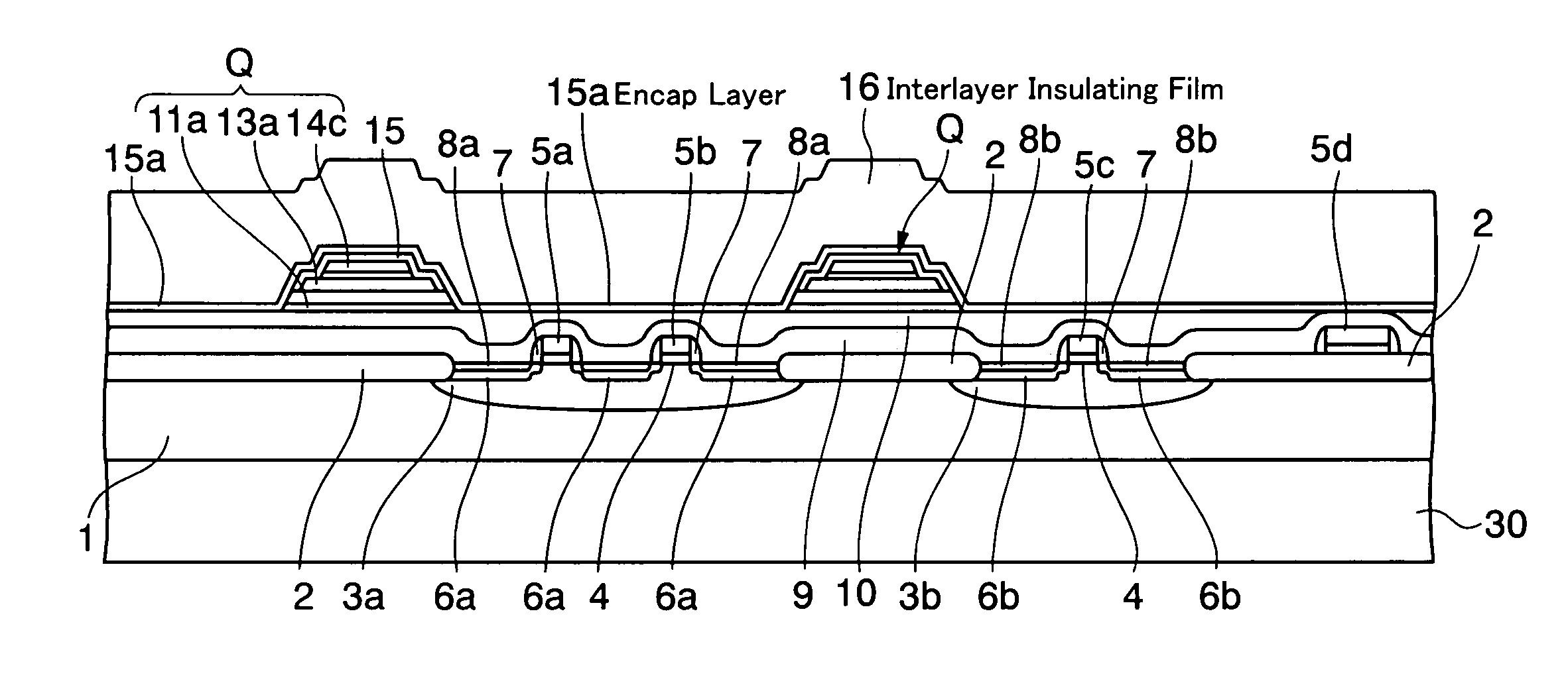
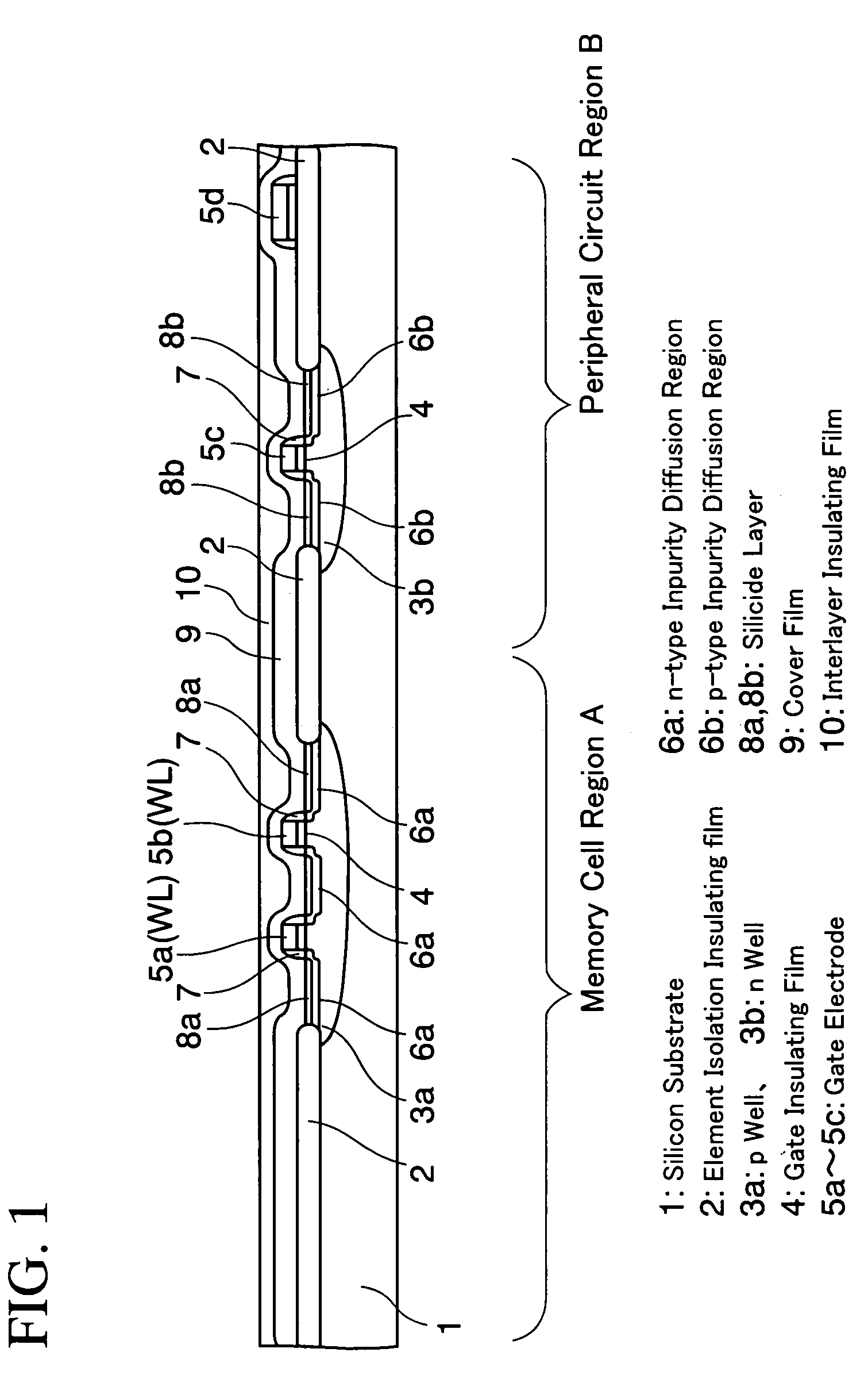
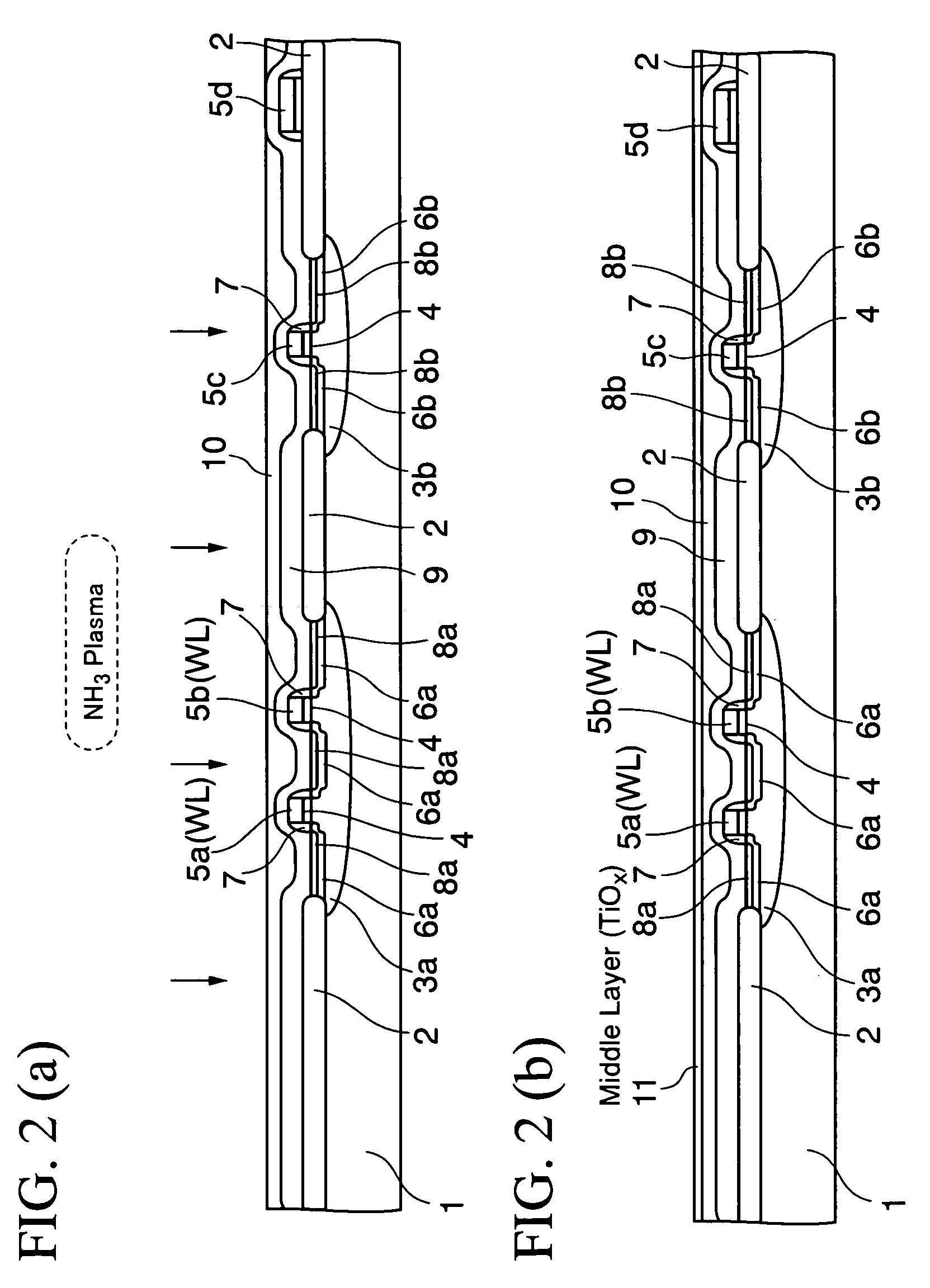
[0035]FIGS. 1 to 11 are the sectional views showing the manufacturing process of the FeRAM of a planar structure according to the embodiments of the present invention.

[0036]Description will be made for the process until the structure shown in FIG. 1 will be formed.

[0037]First, as shown in FIG. 1, an element isolation insulating film 2 is formed on the surface of an n-type or a p-type silicon (semiconductor) substrate 1 by a LOCOS (Local Oxidation of Silicon) method. An STI (Shallow Trench Isolation) structure may be employed other than the structure formed by the LOCOS method.

[0038]After such element isolation insulating film 2 is formed, a p-type impurity and an n-type impurity are selectively introduced in predetermined active regions (transistor forming regions) of a memory cell region A and a peripheral circuit region B of the silicon substrate 1 to form a p-well 3a and an n-well 3b...


PUM


Abstract

A method of manufacturing a semiconductor device comprises the steps of forming a first insulating film 9, 10 above a semiconductor substrate 1; forming a capacitor Q having a lower electrode 11a, a dielectric film 13a, and an upper electrode 14c on the first insulating film 9, 10; forming a second insulating film 15, 15a, 16 coating the capacitor Q; and forming a stress-controlling insulating film 30 on the rear surface of the semiconductor substrate 1 after the second insulating film 15, 15a, 16 have been formed.

Description

CROSS-REFERENCE TO RELATED APPLICATIONS[0001]This application is a continuation of prior International Patent Application No. PCT / JP2002 / 013485, filed Dec. 25, 2002, the entire content of which are incorporated herein by reference.TECHNICAL FIELD[0002]The present invention relates to a method of manufacturing a semiconductor device, more particularly to a method of manufacturing a semiconductor device having capacitors.BACKGROUND ART[0003]There is known a flash memory and an FeRAM (Ferroelectric Random Access Memory) as a non-volatile memory capable of storing information even if a power source is turned off.[0004]The flash memory has a floating gate buried in a gate insulating film of an insulated-gate field effect transistor (IGFET), and stores information by accumulating charges that become storage information in the floating gate. Tunnel current passing through a gate insulating film needs to be flown in order to write and erase information, and thus relatively high voltage is r...

Claims


Application Information

Patent Timeline
Patent Type & Authority Patents(United States)
IPC IPC(8): H01L21/8242H01L21/02H01L21/314H01L21/316H01L21/8246H01L27/115
CPCH01L21/314H01L27/11502H01L27/11507H01L28/57H01L21/31612H01L21/31616H01L28/55H01L28/65H01L21/022H01L21/02271H10B53/30H10B53/00
Inventor SASHIDA, NAOYA
Owner FUJITSU SEMICON LTD
Why Eureka
Try Eureka