Method of production of semiconductor light emission device and method of production of light emission apparatus

a light emission device and light emission technology, applied in the direction of semiconductor lasers, instruments, record information storage, etc., can solve the problem of difficulty in actual circumstances in further reducing the chip size (width) and achieve the effect of improving the uniformity of characteristics, reducing the size of the device, and improving yield

Inactive Publication Date: 2006-07-27
SONY CORP
View PDF3 Cites 19 Cited by
  • Summary
  • Abstract
  • Description
  • Claims
  • Application Information

AI Technical Summary

Benefits of technology

[0017] According to the method of production of the semiconductor light emission device of the present invention, the size of the device can be reduced while maintaining the uniformity of characteristics and yield. Alternatively, according to the method of production of the semiconductor light emission device of the present invention, the uniformity of characteristics and yield can be improved without changing the size of the device. According

Problems solved by technology

It is therefore difficult to further reduce t

Method used


Image

  • Method of production of semiconductor light emission device and method of production of light emission apparatus
  • Method of production of semiconductor light emission device and method of production of light emission apparatus
  • Method of production of semiconductor light emission device and method of production of light emission apparatus

Examples


Embodiment Construction

[0031] Preferred embodiments of the present invention will be described in detail below while referring to the attached figures.

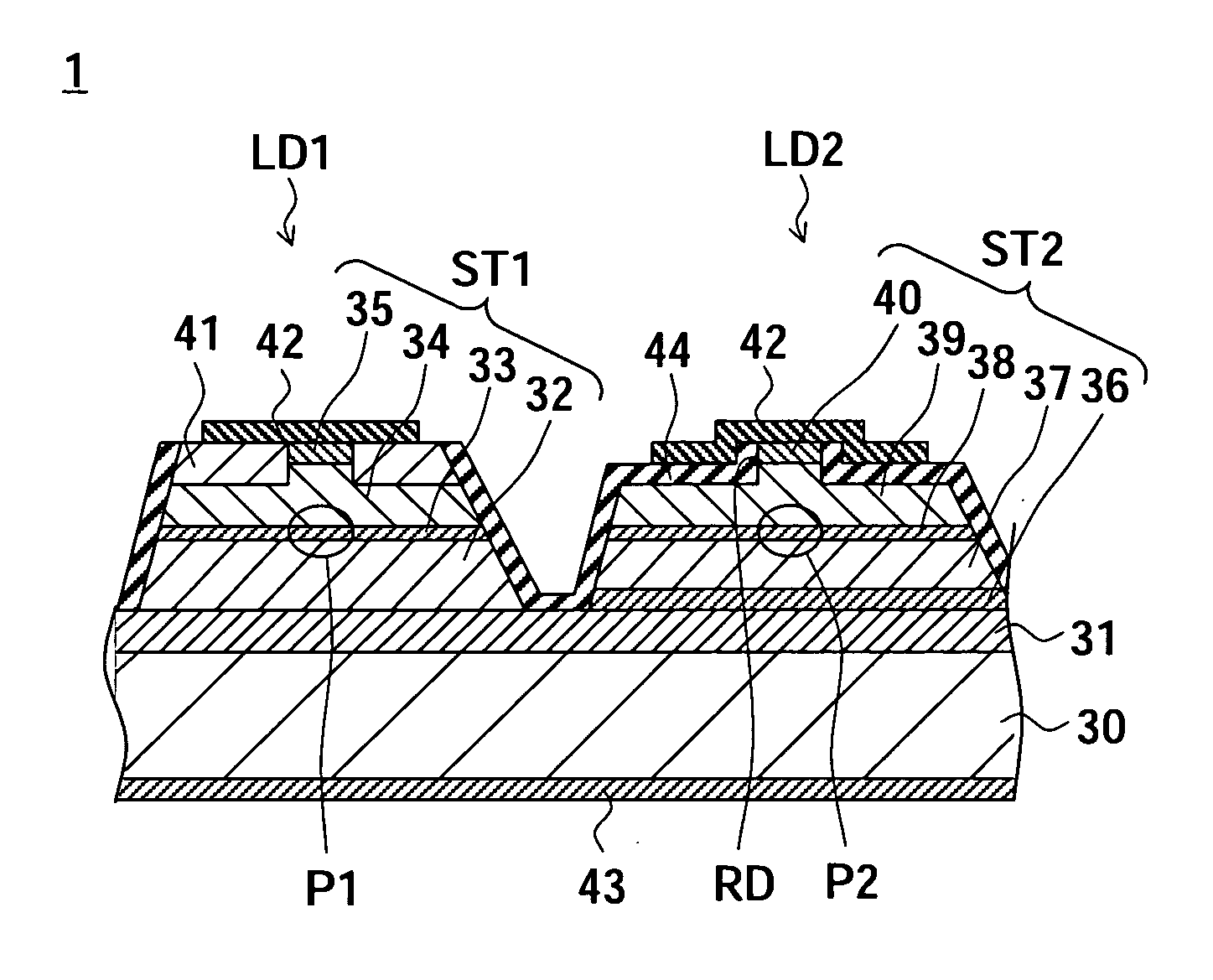
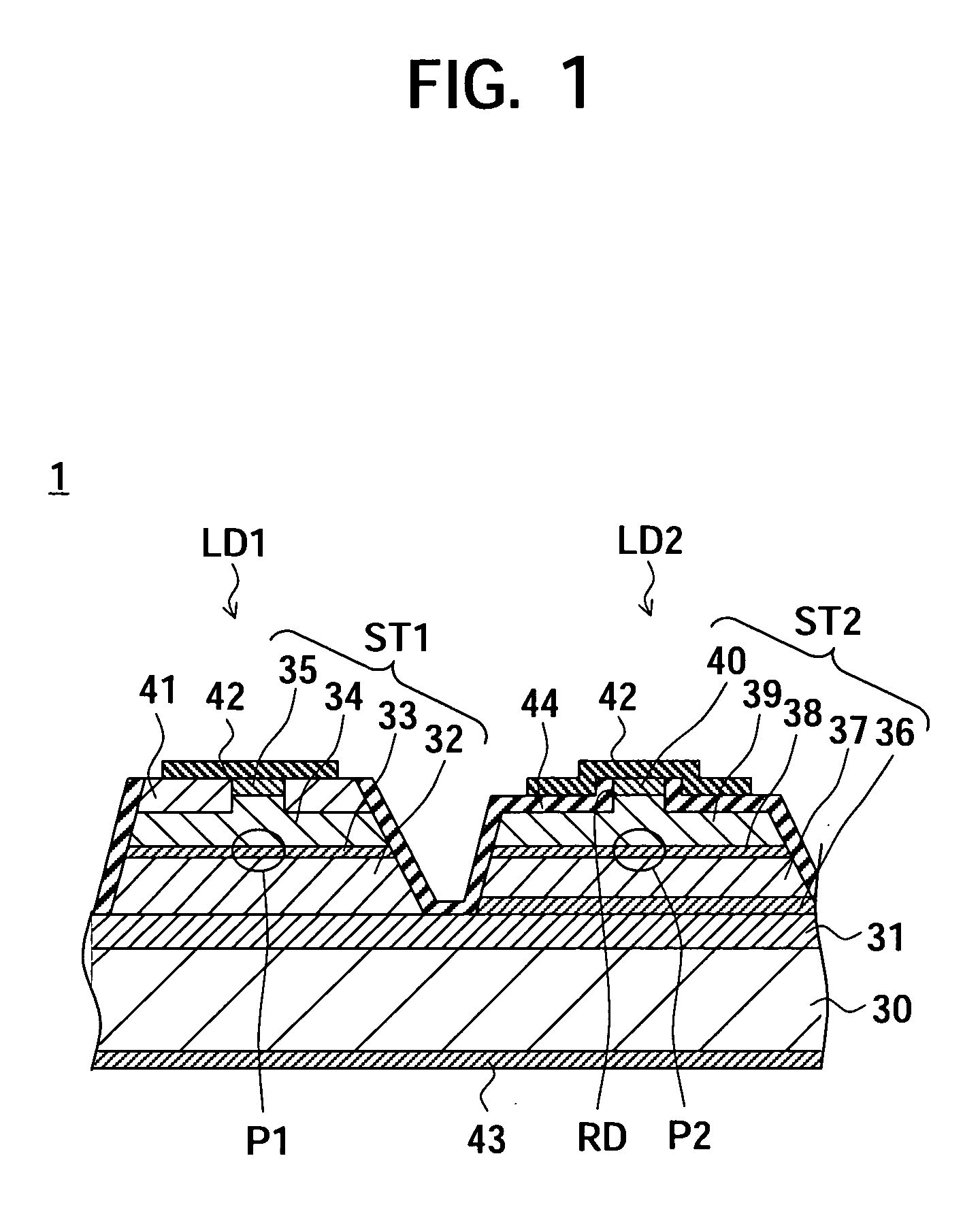
[0032]FIG. 1 is a sectional view of a semiconductor light emission device according to the present embodiment.

[0033] A semiconductor light emission device 1 according to the present embodiment is a monolithic laser diode mounting a laser diode LD1 for a CD (emission wavelength: 780 nm) and a laser diode LD2 for a DVD (emission wavelength: 650 nm) on a single chip and is suitable for constructing a compatible optical pickup apparatus enabling the reproduction of a CD and DVD.

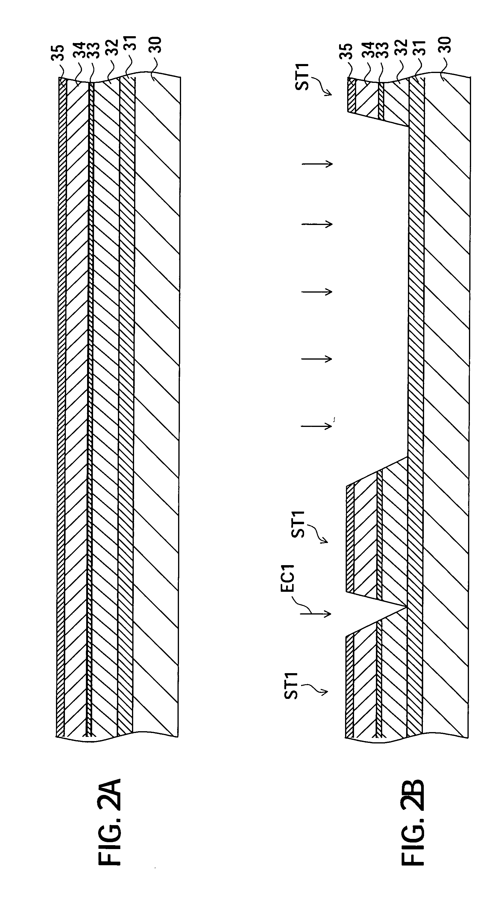
[0034] The first laser diode LD1 includes an n-type substrate 30 made of for example GaAs on which an an n-type buffer layer 31 made of for example GaAs, an n-type cladding layer 32 made of for example AlGaAs, an active layer (multi quantum well structure) 33, a p-type cladding layer 34 made of for example AlGaAs, and a p-type cap layer 35 made of for example GaAs are formed, whereby ...


PUM


Abstract

A method of production of semiconductor light emission devices for forming stripes of two multilayers having different emission wavelengths on a substrate, including the steps of: depositing a first multilayer including an active layer on the substrate; selectively etching the first multilayer to form a plurality of adjoining pairs of stripes of the first multilayer; depositing a second multilayer including an active layer on the substrate and the stripes of the first multilayer; selectively etching the second multilayer to form a plurality of adjoining pairs of stripes of the second multilayer on the substrate between the stripes of the first multilayer; and dividing the substrate between adjoining pairs of stripes of the first multilayer and between adjoining pairs of stripes of the second multilayer to divide it into semiconductor light emission devices provided with a stripe of the first multilayer and the second multilayer having different emission wavelengths.

Description

CROSS REFERENCES TO RELATED APPLICATIONS [0001] The present invention contains subject matter related to Japanese Patent Application No. 2005-018368 and No. 2005-018369 filed in the Japan Patent Office on Jan. 26, 2005, the entire contents of which being incorporated herein by reference. BACKGROUND OF THE INVENTION [0002] 1. Field of the Invention [0003] The present invention relates to a method of production of a semiconductor light emission device and a method of production of a light emission apparatus, more particularly relates to a method of production of a semiconductor light emission device provided with a plurality of multilayers emitting lights having different wavelengths and a light emission apparatus mounting the semiconductor light emission device in a package. [0004] 2. Description of the Related Art [0005] In general, an apparatus for reading (reproducing) information recorded on a compact disc (CD), digital versatile disc (DVD), mini disc (MD), or other optical recor...

Claims


Application Information

Patent Timeline
IPC IPC(8): H01L21/00
CPCB82Y20/00G11B7/1275G11B7/22G11B2007/0006H01L27/153H01S5/0202H01S5/02212H01S5/0224H01S5/0425H01S5/0683H01S5/34313H01S5/34326H01S5/4031H01S5/4087H01S5/04256H01S5/0234
Inventor NEMOTO, KAZUHIKO
Owner SONY CORP
Why Eureka
Try Eureka