Method of manufacturing liquid crystal device, liquid crystal device, and electronic apparatus

Active Publication Date: 2006-06-29
138 EAST LCD ADVANCEMENTS LTD
View PDF23 Cites 23 Cited by
  • Summary
  • Abstract
  • Description
  • Claims
  • Application Information

AI Technical Summary

Benefits of technology

[0079] According to this configuration, an electronic apparatus having a display un

Problems solved by technology

When liquid crystal is filled in such a manner, however, the liquid crystal injection process takes an extremely long time.
In particular, when a large substrate whose diagonal is more than one meter is used, it takes more than one day to entirely fill the substrate with liquid crystal.
For example, if the dropping amount is excessively small, the cell gap is thin, and thus air bubbles tend to occur.
Further, if the dropping amount is excessively large, the cell gap is thick, and unevenness of the cell gap tends to occur.
In addition, the inventors have founded that, in the method of forming the sealant by use of the dispenser, in general, a defective cell gap tends to occur.
This is because, when the size is excessively large, the cell gap is thickened, such that display unevenness occurs, and, when the cell gap is minute, liquid crystal may leak from that portion, such that reliability is degraded.
In this method, however, the control of the dispenser is very complex, it takes a long time for drawing, the seal shape tends to be varied due to a variation in the amount of a residual sealant in the dispenser or a variation in viscosity between different lots of the sealant,

Method used


Image

  • Method of manufacturing liquid crystal device, liquid crystal device, and electronic apparatus
  • Method of manufacturing liquid crystal device, liquid crystal device, and electronic apparatus
  • Method of manufacturing liquid crystal device, liquid crystal device, and electronic apparatus

Examples


Example

First Embodiment

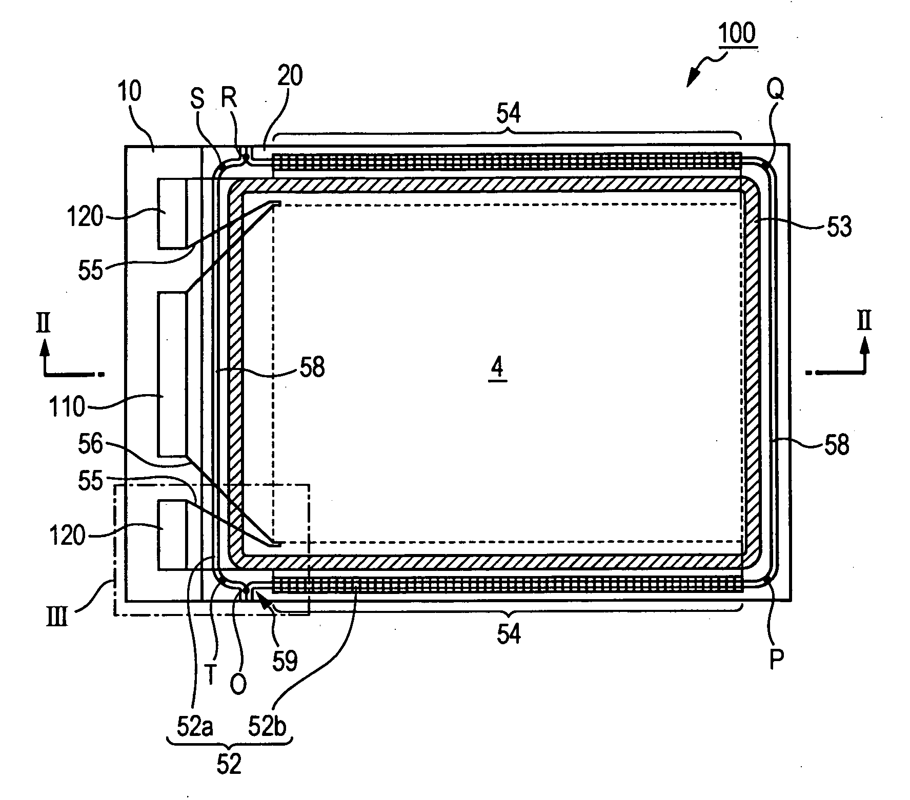
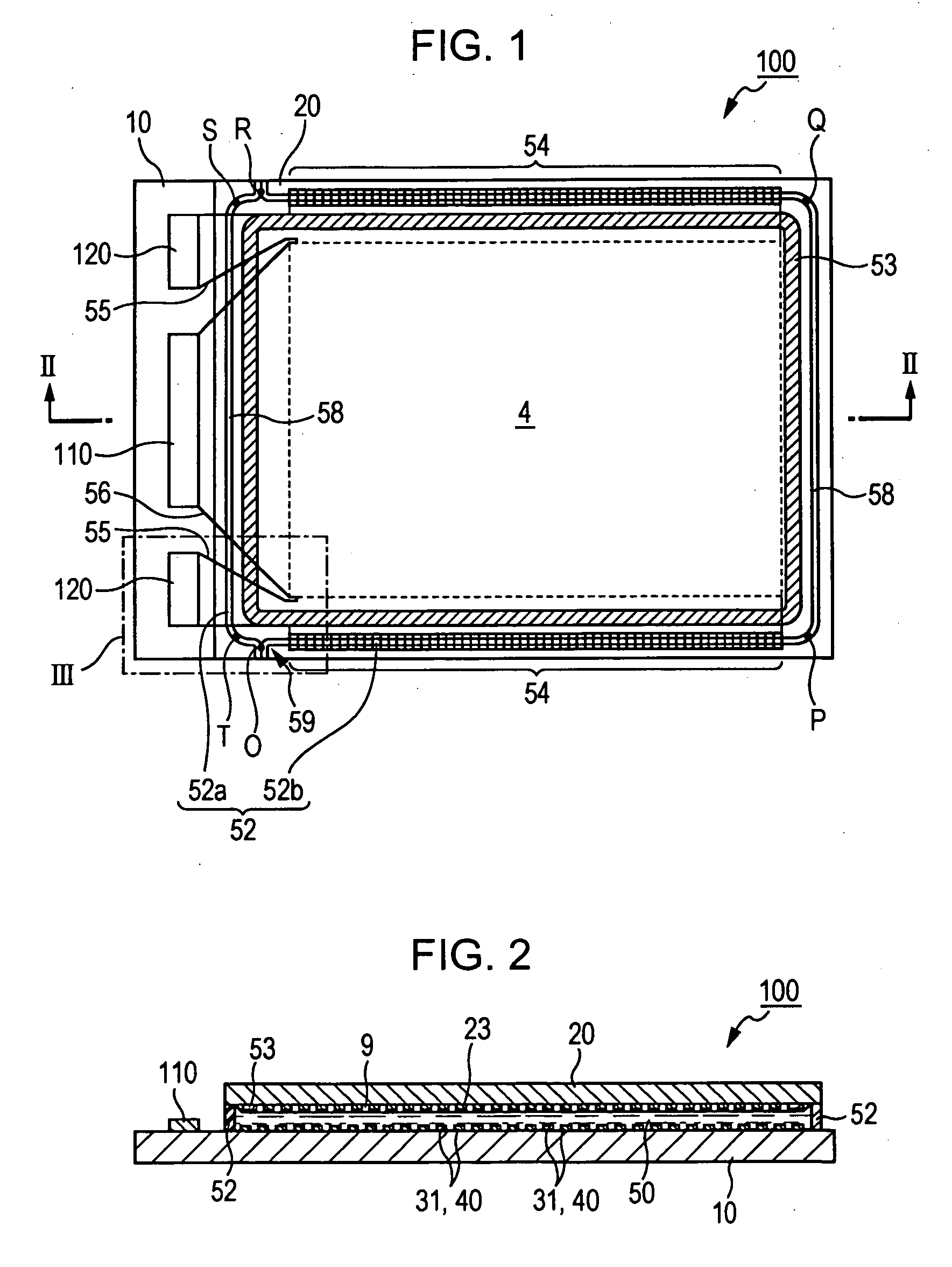
[0151] First, a liquid crystal device according to a first embodiment of the invention will be described.

[0152] The liquid crystal device of the present embodiment described below is an example of an active matrix type liquid crystal device which uses a thin film diode (hereinafter, referred to as TFD) as a switching element. The liquid crystal device of the present invention is also a transmissive liquid crystal device in which transmissive display can be performed.

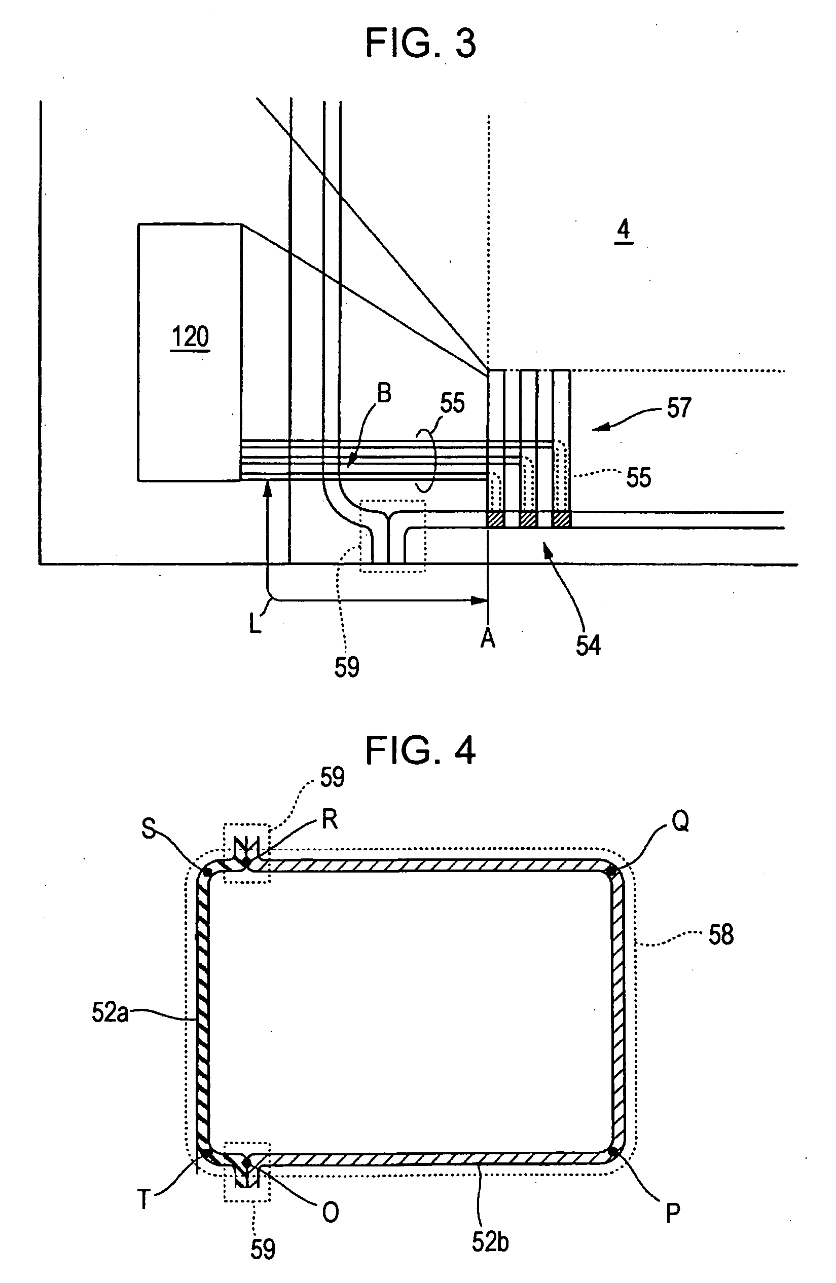
[0153]FIG. 1 is a plan view of individual constituent parts of the liquid crystal device according to the present embodiment as viewed from a counter substrate. FIG. 2 is a cross-sectional view taken along the line II-II of FIG. 1. Further, FIG. 3 is a plan view showing a region denoted by a symbol C in FIG. 1 on a magnified scale. FIG. 4 is a plan view illustrating the configuration of a sealing member in detail. FIG. 5 is an equivalent circuit diagram of various elements, wiring lines, and the like i...

Example

Second Embodiment

[0295]FIG. 19 is a diagram illustrating a manufacturing method of a liquid crystal device according to the second embodiment of the invention. Further, FIG. 19 is a plan view illustrating a method of forming a sealing member 52. In addition, FIG. 19 is a diagram showing a portion indicated by a symbol F in FIG. 18B on a magnified scale.

[0296] In the first embodiment, the first sealing layer 59a and the second sealing layer 59b are configured to have the curved portions 59c. On the other hand, in the present embodiment, the first sealing layer 59a and the second sealing layer 59b are configured to have inclined portions 59d. Then, as described above, when the mother substrate 10′ for a TFD substrate and the mother substrate 20′ for a counter substrate are bonded to each other, the first sealing layer 59a and the second sealing layer 59b are crushed and joined, such that the junction portion 59 shown in FIG. 4 is formed.

[0297] Next, the shape sizes of the first sea...

Example

Third Embodiment

[0301]FIG. 20 is a diagram illustrating a manufacturing method of a liquid crystal device according to a third embodiment of the invention. Further, FIG. 20 is a plan view showing respective constituent parts of the liquid crystal device as viewed from the counter substrate. FIG. 21 is a plan view showing a region indicated by a symbol C of FIG. 20 on a magnified scale. FIG. 22 is a plan view specifically illustrating the configuration of the sealing member.

[0302] As shown in FIGS. 20 to 22, in the liquid crystal device 100 of the present embodiment, the insulating sealing member (second sealing member) 52a is linearly formed in a vertical direction of the paper. Further, at points O and R, the insulating sealing member 52a and the conductive sealing member (first sealing member) 52b are connected to each other.

[0303] Further, the insulating sealing member 52a and the conductive sealing member 52b are formed in a pattern shown in FIG. 22, and thus a single ring-sh...


PUM

PropertyMeasurementUnit
Fractionaaaaaaaaaa
Lengthaaaaaaaaaa
Lengthaaaaaaaaaa

Abstract

A method of manufacturing a liquid crystal device having a first substrate and a second substrate facing each other with a liquid crystal layer interposed therebetween, and a sealing member formed in a peripheral portion of at least one of the substrates. The method includes forming the sealing member, disposing the liquid crystal layer inside the sealing member, and bonding the first substrate to the second substrate. In forming the sealing member, a ring-shaped portion that seals the liquid crystal layer inside the sealing member, a first sealing layer and a second sealing layer that face each other to be separated from each other are formed. In the bonding of the first substrate to the second substrate, a junction portion is formed in which the first and second sealing layers are pressed and joined outside the sealing member so as to form the ring-shaped portion.

Description

RELATED APPLICATIONS [0001] This application claims priority to Japanese Patent Application No. 2004-375697 filed Dec. 27, 2004 which is hereby expressly incorporated by reference in its entirety. BACKGROUND [0002] 1. Technical Field [0003] The present invention relates to a method of manufacturing a liquid crystal device, to a liquid crystal device, and an electronic apparatus. [0004] 2. Related Art [0005] In an electronic apparatus, such as a cellular phone or the like, an electro-optical device, such as a liquid crystal device or the like, is used as a color image display unit. The liquid crystal device has a pair of substrates with a liquid crystal layer interposed therebetween. In order to form the liquid crystal device, first, a sealant (sealing material) is coated in a peripheral portion of a surface of one substrate. At that time, a liquid crystal injection hole is formed at a part of the sealant. Next, spacers are sprayed inside the sealant, and then the other substrate is ...

Claims


Application Information

Patent Timeline
IPC IPC(8): G02F1/1339
CPCG02F1/1339G02F1/1341G02F1/13394G02F2202/023G02F1/13415
Inventor MOMOSE, YOICHIHASEGAWA, SATOSHI
Owner 138 EAST LCD ADVANCEMENTS LTD
Why Eureka
Try Eureka