Semiconductor device manufacturing method

a manufacturing method and semiconductor technology, applied in the direction of semiconductor devices, basic electric elements, electrical appliances, etc., can solve the problem of not being able to continue miniaturizing semiconductor devices, and achieve the effects of low cost, high accuracy, and uniformity

Inactive Publication Date: 2011-05-05
TOKYO ELECTRON LTD
View PDF12 Cites 19 Cited by
  • Summary
  • Abstract
  • Description
  • Claims
  • Application Information

AI Technical Summary

Benefits of technology

[0060]According to the present invention, on the occasion when a semiconductor device is manufactured by using the double patterning method including the SWT method, even number patterns and odd number patterns can be formed in a lump at low costs, and, even in a case where an area of fine pattern density and an area of coarse pattern density are mixed in patterns used as hard masks, CD of the patterns can be maintained uniform at high accuracy.

Problems solved by technology

However, along with miniaturization processing so that a most advanced design rule becomes 45 nm and further becomes 32 nm, it becomes not possible to continue miniaturization of a semiconductor device only by photolithography in which a photoresist film is exposed by using an optical system and patterns are formed through development.

Method used


Image

  • Semiconductor device manufacturing method
  • Semiconductor device manufacturing method
  • Semiconductor device manufacturing method

Examples


first embodiment

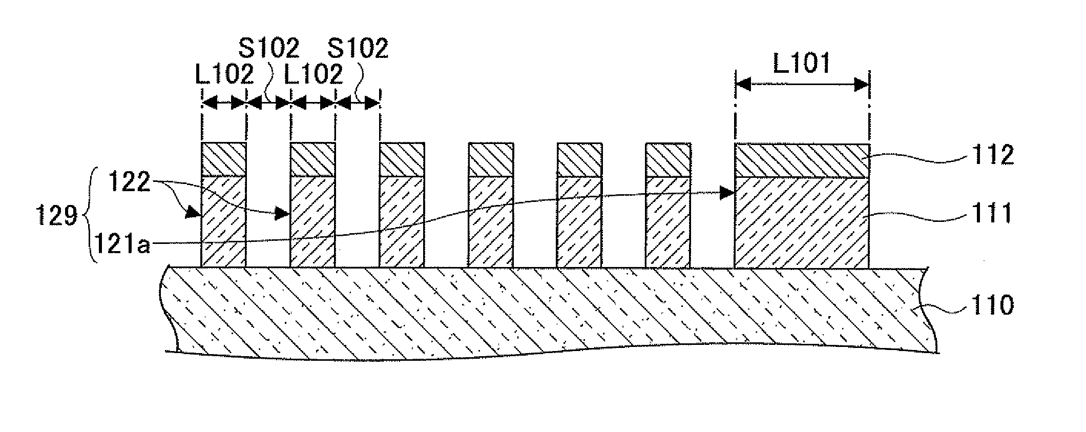
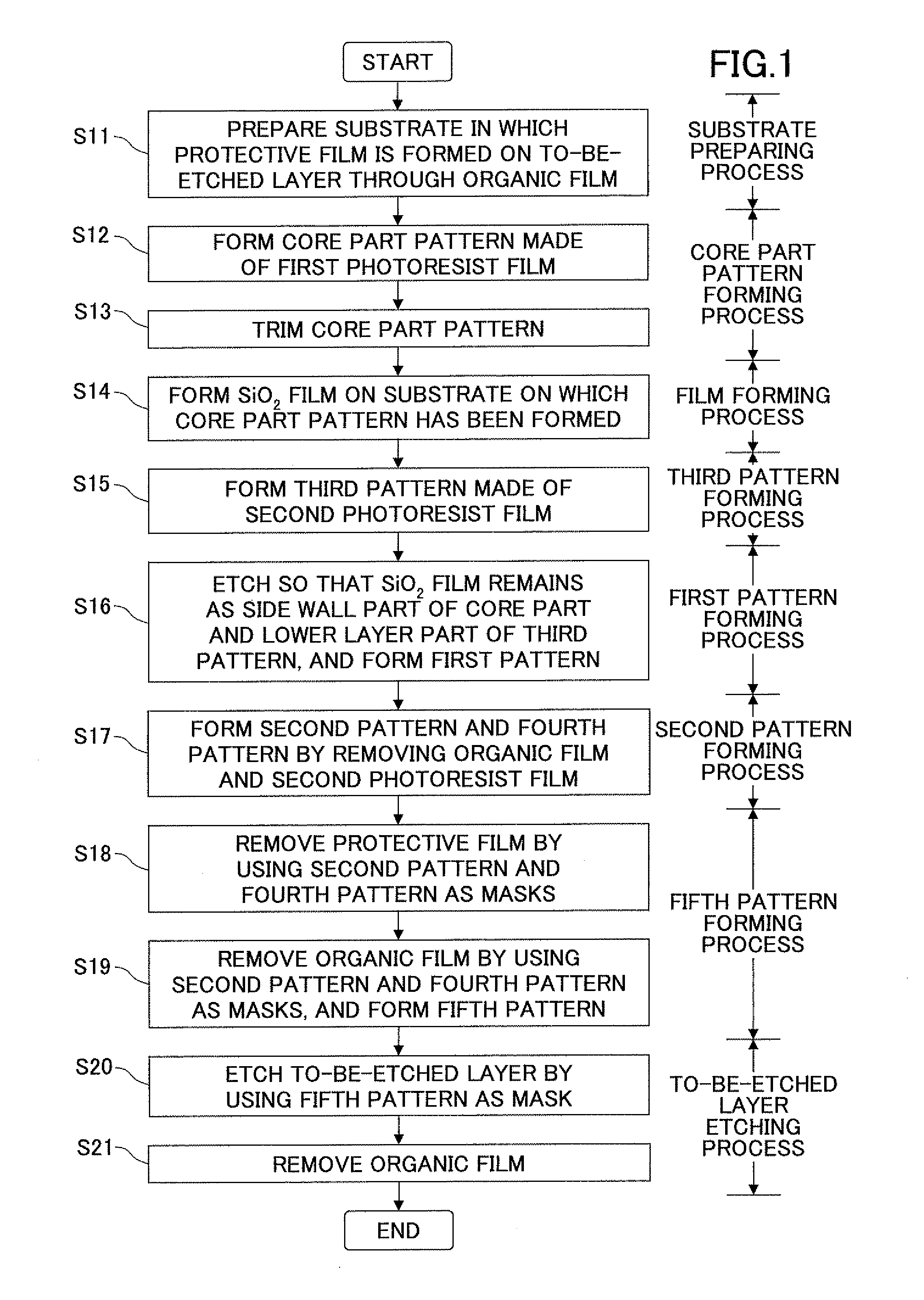
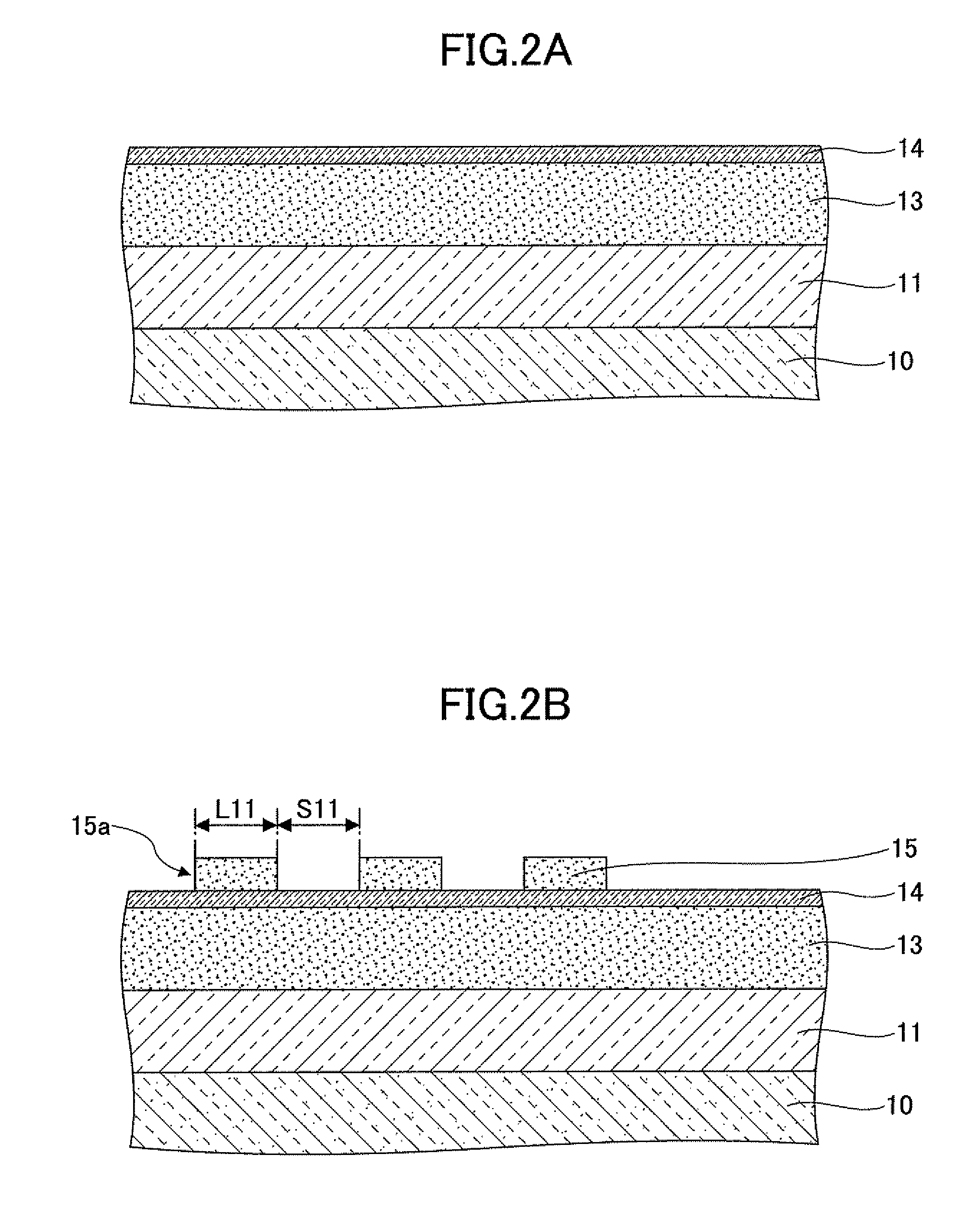
[0254]With reference to FIGS. 1 through 2K, a semiconductor device manufacturing method according to a first embodiment of the present invention will be described.

[0255]Below, a first photoresist film, a core part pattern, a core part pattern forming process, a film forming process, a first pattern, a first pattern forming process, a second photoresist film, a third pattern, a third pattern forming process, a fourth pattern, a second pattern, and a second pattern forming process in the present embodiment and respective variant embodiments of the present embodiment correspond to a first organic film, a first organic film pattern, a first organic film pattern forming process, a silicon oxide film forming process, a first mask pattern, a first mask pattern forming process, a second organic film, a second organic film pattern, a second organic film pattern forming process, a second mask pattern, a third mask pattern, and a third mask pattern forming process according to the present inve...

second embodiment

[0374]With reference to FIGS. 9 through 10L, a semiconductor device manufacturing method according to a second embodiment of the present invention will be described.

[0375]Below, an organic film, a core part pattern, a core part pattern forming process, a film forming process, a first pattern, a first pattern forming process, a second photoresist film, a third pattern, a third pattern forming process, a predetermined pattern of the first pattern, a first pattern forming process, a second pattern, a second pattern forming process, in the present embodiment and respective variant embodiments of the present embodiment correspond to a first organic film, a first organic film pattern, a first organic film pattern forming process, a silicon oxide film forming process, a first mask pattern, a first mask pattern forming process, a second organic film, a second organic film pattern, a second organic film pattern forming process, a second mask pattern, a second mask pattern forming process, a ...

first variant embodiment

of Second Embodiment

[0429]Next, with reference to FIGS. 11A through 11L, a semiconductor device manufacturing method in a first variant embodiment of the second embodiment according to the present invention will be described.

[0430]FIGS. 11A through 11L illustrate processes of the semiconductor device manufacturing method in the present variant embodiment, and are sectional views diagrammatically showing structures of the semiconductor device in the respective processes. It is noted that in the description below, the same reference numerals are given to the parts already described above, and description may be omitted (also the same in variant embodiments and embodiments below).

[0431]The semiconductor device manufacturing method according to the present variant embodiment is different from the semiconductor device manufacturing method according to the second embodiment in that the second to-be-etched layer is a silicon nitride layer.

[0432]With reference to FIGS. 11A through 11L, diff...


PUM


Abstract

A semiconductor device manufacturing method includes a process of forming a first organic film pattern on a to-be-etched layer on a substrate, a process of forming a silicon oxide film coating the first organic film pattern in an isotropic manner, a process of etching the silicon oxide film to form a first mask pattern in such a manner to cause the width of the line part of the first organic film pattern to have a fixed proportion with respect to a thickness of the silicon oxide film that coats a surface of the line part in the isotropic manner, a process of forming a second organic film pattern coating the silicon oxide film, a process of forming a second mask pattern that includes the silicon oxide film on a side face part in an area that is coated by the second organic film pattern, and a process of, in an area other than the area that is coated by the second organic film pattern, forming a third mask pattern in which an even number of the silicon oxide films are arranged.

Description

TECHNICAL FIELD[0001]The present invention relates to a semiconductor device manufacturing method, a program for performing the manufacturing method and a recording medium that records the program, and, in particular, to a semiconductor device manufacturing method in which a semiconductor device is manufactured by using a double patterning method including a SWT method, a program for performing the manufacturing method and a recording medium that records the program.BACKGROUND ART[0002]In the prior art, in a semiconductor device manufacturing process, an etching process such as plasma etching is performed on a substrate such as a semiconductor wafer, and fine circuit patterns and so forth are formed. In the etching process, through a photolithography process using a photoresist, an etching mask is formed.[0003]Resolution in the photolithography is expressed by k1×λ / NA by using a constant k1 depending on a process condition and an optical system, a wavelength λ of exposure light, and...

Claims


Application Information

Patent Timeline
Patent Type & Authority Applications(United States)
IPC IPC(8): H01L21/302
CPCH01L21/0337H01L21/0338H01L27/11521H01L21/76816H01L21/31144H10B41/30H01L21/0274
Inventor YATSUDA, KOICHINISHIMURA, EIICHI
Owner TOKYO ELECTRON LTD
Why Eureka
Try Eureka