Method for making a semiconductor device having a high-k gate dielectric layer and a metal gate electrode

a metal gate electrode and dielectric layer technology, applied in the direction of semiconductor devices, basic electric elements, electrical appliances, etc., can solve the problems of large variation in the thickness of the underlying oxide layer may be significant, and the gate leakage current of the very thin gate dielectric made from silicon dioxide is unacceptabl

Active Publication Date: 2007-01-02
TAHOE RES LTD
View PDF40 Cites 107 Cited by
  • Summary
  • Abstract
  • Description
  • Claims
  • Application Information

AI Technical Summary

Problems solved by technology

MOS field-effect transistors with very thin gate dielectrics made from silicon dioxide may experience unacceptable gate leakage currents.
Because, however, such a dielectric may not be compatible with polysilicon, it may be desirable to use metal gate electrodes in devices that include high-k gate dielectrics.
If the workfunction metals polish slowly, it may require a relatively long overpolish step to completely remove them.
When such an overpolish step is not selective to the underlying high-k gate dielectric layer, significant lot to lot or wafer to wafer variation in the thickness of an underlying oxide layer may result.
In some cases, severe reduction in oxide thickness may occur over parts of a wafer by the time the polishing operation is completed.

Method used


Image

  • Method for making a semiconductor device having a high-k gate dielectric layer and a metal gate electrode
  • Method for making a semiconductor device having a high-k gate dielectric layer and a metal gate electrode
  • Method for making a semiconductor device having a high-k gate dielectric layer and a metal gate electrode

Examples


Embodiment Construction

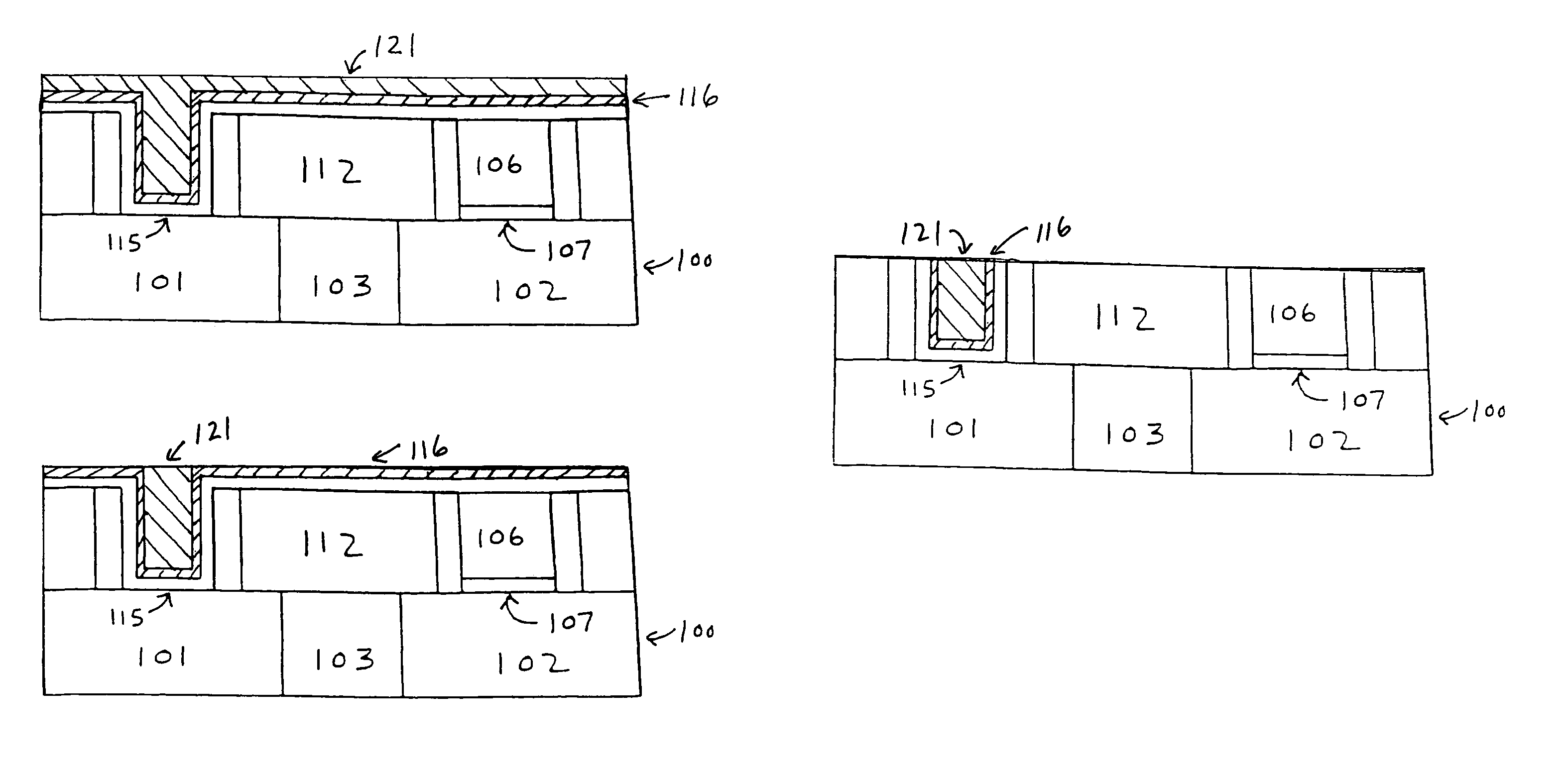
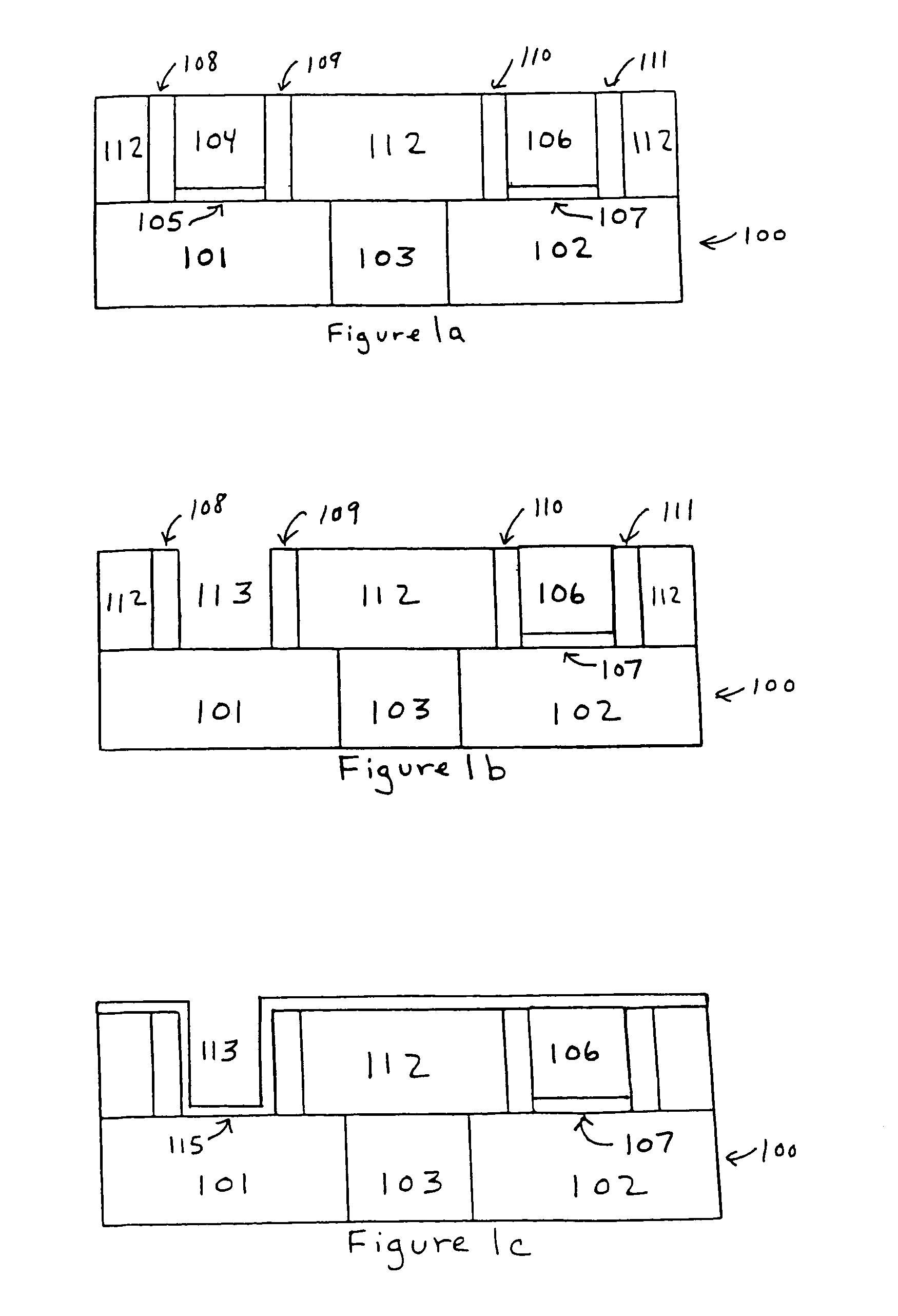
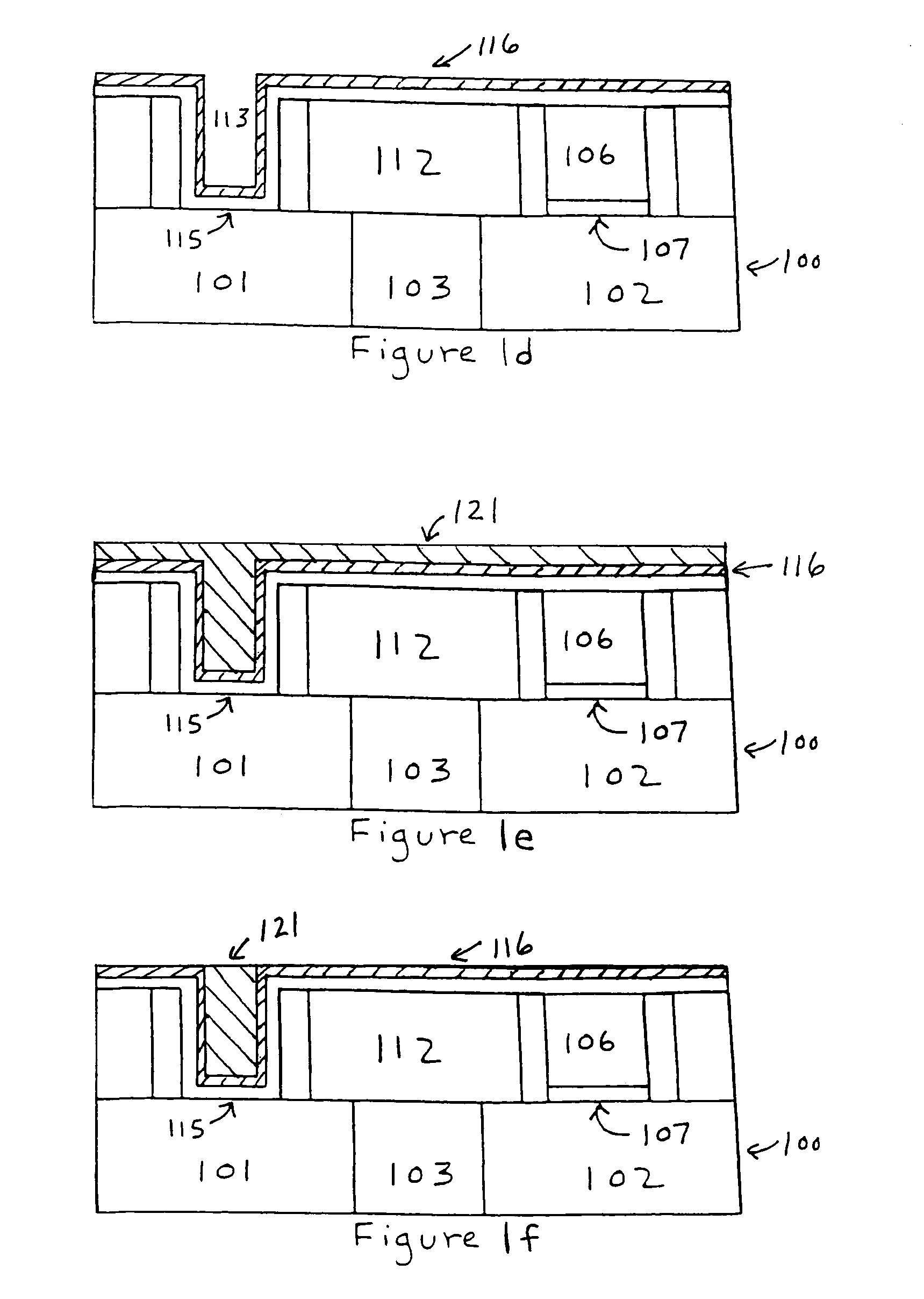
[0010]A method for making a semiconductor device is described. That method comprises forming a dielectric layer on a substrate, forming a trench within the dielectric layer, and forming a high-k gate dielectric layer within the trench. After forming a first metal layer on the high-k gate dielectric layer, a second metal layer is formed on the first metal layer. At least part of the second metal layer is removed from above the dielectric layer using a polishing step, and additional material is removed from above the dielectric layer using an etch step.

[0011]In the following description, a number of details are set forth to provide a thorough understanding of the present invention. It will be apparent to those skilled in the art, however, that the invention may be practiced in many ways other than those expressly described here. The invention is thus not limited by the specific details disclosed below.

[0012]FIGS. 1a–1j illustrate structures that may be formed, when carrying out an emb...


PUM

PropertyMeasurementUnit
workfunctionaaaaaaaaaa
thickaaaaaaaaaa

Abstract

A method for making a semiconductor device is described. That method comprises forming a dielectric layer on a substrate, forming a trench within the dielectric layer, and forming a high-k gate dielectric layer within the trench. After forming a first metal layer on the high-k gate dielectric layer, a second metal layer is formed on the first metal layer. At least part of the second metal layer is removed from above the dielectric layer using a polishing step, and additional material is removed from above the dielectric layer using an etch step.

Description

FIELD OF THE INVENTION[0001]The present invention relates to methods for making semiconductor devices, in particular, semiconductor devices that include metal gate electrodes.BACKGROUND OF THE INVENTION[0002]MOS field-effect transistors with very thin gate dielectrics made from silicon dioxide may experience unacceptable gate leakage currents. Forming the gate dielectric from certain high-k dielectric materials, instead of silicon dioxide, can reduce gate leakage. Because, however, such a dielectric may not be compatible with polysilicon, it may be desirable to use metal gate electrodes in devices that include high-k gate dielectrics.[0003]When making a CMOS device that includes metal gate electrodes, a replacement gate process may be used to form gate electrodes from different metals. In that process, a first polysilicon layer, bracketed by a pair of spacers, is removed to create a first trench between the spacers. A first workfunction metal is deposited within the trench. A second...

Claims


Application Information

Patent Timeline
Patent Type & Authority Patents(United States)
IPC IPC(8): H01L21/302H01L21/336H01L21/8234H01L21/8238
CPCH01L21/28185H01L21/28194H01L21/28229H01L21/82345H01L21/823462H01L21/823842H01L21/823857H01L29/4966H01L29/513H01L29/517H01L29/66545H01L21/18
Inventor BRASK, JUSTIN K.BARNS, CHRIS E.DOCZY, MARK L.SHAH, UDAYKAVALIEROS, JACKMETZ, MATTHEW V.DATTA, SUMANMILLER, ANNE E.CHAU, ROBERT S.
Owner TAHOE RES LTD
Why Eureka
Try Eureka