CVD nanoporous silica low dielectric constant films

a technology of nanoporous silica and dielectric constant, applied in the direction of chemical vapor deposition coating, semiconductor/solid-state device details, coatings, etc., can solve the problems of affecting the overall performance of the device, and insufficient etch stop layer material

Inactive Publication Date: 2001-01-09
APPLIED MATERIALS INC
View PDF28 Cites 410 Cited by
  • Summary
  • Abstract
  • Description
  • Claims
  • Application Information

AI Technical Summary

Problems solved by technology

The high temperatures at which some thermal CVD processes operate can damage device structures having layers previously formed on the substrate.
However, the barrier / liner layers typically have dielectric constants that are significantly greater than 4.0, and the high dielectric constants result in a combined insulator that may not significantly reduce the dielectric constant.
Furthermore, known low k dielectric materials generally have low oxide content which makes the material inadequate as an etch stop layer during etching of vias and / or interconnects.
This may lead to crosstalk and / or resistance-capacitance (RC) delay that degrades the overall performance of the device.
The '570 patent does not identify process conditions for making barrier layers having low dielectric constants or for making etch stop layers having high oxide contents.

Method used


Image

  • CVD nanoporous silica low dielectric constant films
  • CVD nanoporous silica low dielectric constant films
  • CVD nanoporous silica low dielectric constant films

Examples


examples

The following examples demonstrate deposition of a nano-porous silicon oxide based film having dispersed microscopic gas voids. This example is undertaken using a chemical vapor deposition chamber, and in particular, a CENTURA "DLK" system fabricated and sold by Applied Materials, Inc., Santa Clara, Calif.

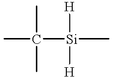
Reactive Silicon Compounds Having Silicon Hydride Groups (Hypothetical)

A nano-porous silicon oxide based film is deposited at a chamber pressure of 1.0 Torr and temperature of 0.degree. C. from reactive gases which are vaporized and flown into the reactor as follows:

The substrate is positioned 600 mil from the gas distribution showerhead and the reactive gases are introduced for 2 minutes. The substrate is then heated over a time period of 10 minutes, raising the temperature of the substrate by 50.degree. C. / min to a temperature of 400.degree. C. to cure and anneal the nano-porous silicon oxide based film.

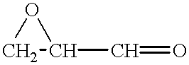
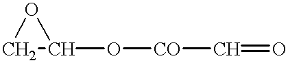
Reactive Silicon Compounds Having Thermally Labile Organic Groups (Hypothetic...


PUM

PropertyMeasurementUnit
temperatureaaaaaaaaaa
feature sizesaaaaaaaaaa

Abstract

A method and apparatus for depositing nano-porous low dielectric constant films by reaction of a silicon hydride containing compound or mixture optionally having thermally labile organic groups with a peroxide compound on the surface of a substrate. The deposited silicon oxide based film is annealed to form dispersed microscopic voids that remain in a nano-porous silicon oxide based film having a foam structure. The nano-porous silicon oxide based films are useful for filling gaps between metal lines with or without liner or cap layers. The nano-porous silicon oxide based films may also be used as an intermetal dielectric layer for fabricating dual damascene structures. Preferred nano-porous silicon oxide based films are produced by reaction of 1,3,5-trisilanacyclohexane, bis(formyloxysilano)methane, or bis(glyoxylylsilano)methane and hydrogen peroxide followed by a cure/anneal that includes a gradual increase in temperature.

Description

BACKGROUND OF THE DISCLOSURE1. Field of the InventionThe present invention relates to the fabrication of integrated circuits. More particularly, the invention relates to a process and apparatus for depositing dielectric layers on a substrate.2. Background of the InventionOne of the primary steps in the fabrication of modern semiconductor devices is the formation of metal and dielectric films on a substrate by chemical reaction of gases. Such deposition processes are referred to as chemical vapor deposition or CVD. Conventional thermal CVD processes supply reactive gases to the substrate surface where heat-induced chemical reactions take place to produce a desired film. The high temperatures at which some thermal CVD processes operate can damage device structures having layers previously formed on the substrate. A preferred method of depositing metal and dielectric films at relatively low temperatures is plasma-enhanced CVD (PECVD) techniques such as described in U.S. Pat. No. 5,362,...

Claims


Application Information

Patent Timeline
Patent Type & Authority Patents(United States)
IPC IPC(8): H01L21/02H01L21/70H01L21/768H01L21/316C23C16/40H01L23/522
CPCH01L21/02126H01L21/02203H01L21/02271H01L21/02304H01L21/02362H01L21/31695H01L21/7681H01L21/76829H01L21/76832H01L21/76834H01L21/76835B82Y40/00
Inventor MANDAL, ROBERT P.CHEUNG, DAVIDYAU, WAI-FAN
Owner APPLIED MATERIALS INC
Why Eureka
Try Eureka