Deposition of silicon dioxide on hydrophobic surfaces

a technology of hydrophobic surface and silicon dioxide, which is applied in the direction of chemical vapor deposition coating, coating, metallic material coating process, etc., can solve the problems of difficult control, difficult deposition of ultra thin, uniform and continuous barrier layer on the low-k surface, and difficult development of silicon dioxide process for deposition on hydrophobic surface without destroying hydrophobicity

Inactive Publication Date: 2012-10-18
ASM IP HLDG BV
View PDF5 Cites 371 Cited by
  • Summary
  • Abstract
  • Description
  • Claims
  • Application Information

AI Technical Summary

Problems solved by technology

However, silicon dioxide processes for deposition on hydrophobic surfaces without destroying the hydrophobicity have been difficult to develop.
The porosity, however, makes it very challenging to deposit ultra thin, uniform and continuous barrier layers on the low-k surface.
However, the oxidation process (Si—CH3 to Si—OH) either with O2-plasma or oxygen containing plasma or ozone can be difficult to control and as a result it is difficult to oxidize just the top-most surface layer.
Rather, oxidation is likely to take place deep in the porous low-k layer as well, leading to an undesired increase in the k-value.
This oxidation has restricted the use of ALD for pore-sealing purposes and for deposition of SiO2 on hydrophobic surfaces generally.

Method used


Image

  • Deposition of silicon dioxide on hydrophobic surfaces
  • Deposition of silicon dioxide on hydrophobic surfaces
  • Deposition of silicon dioxide on hydrophobic surfaces

Examples


example 1

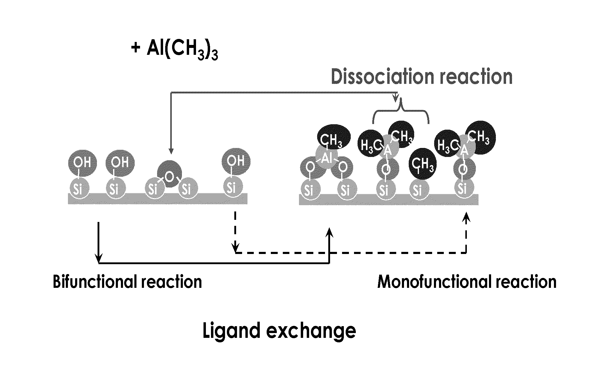
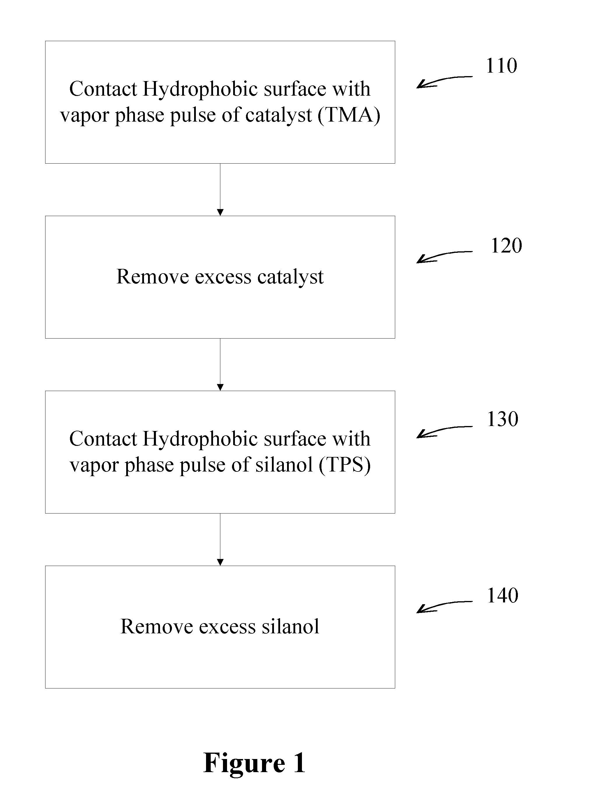
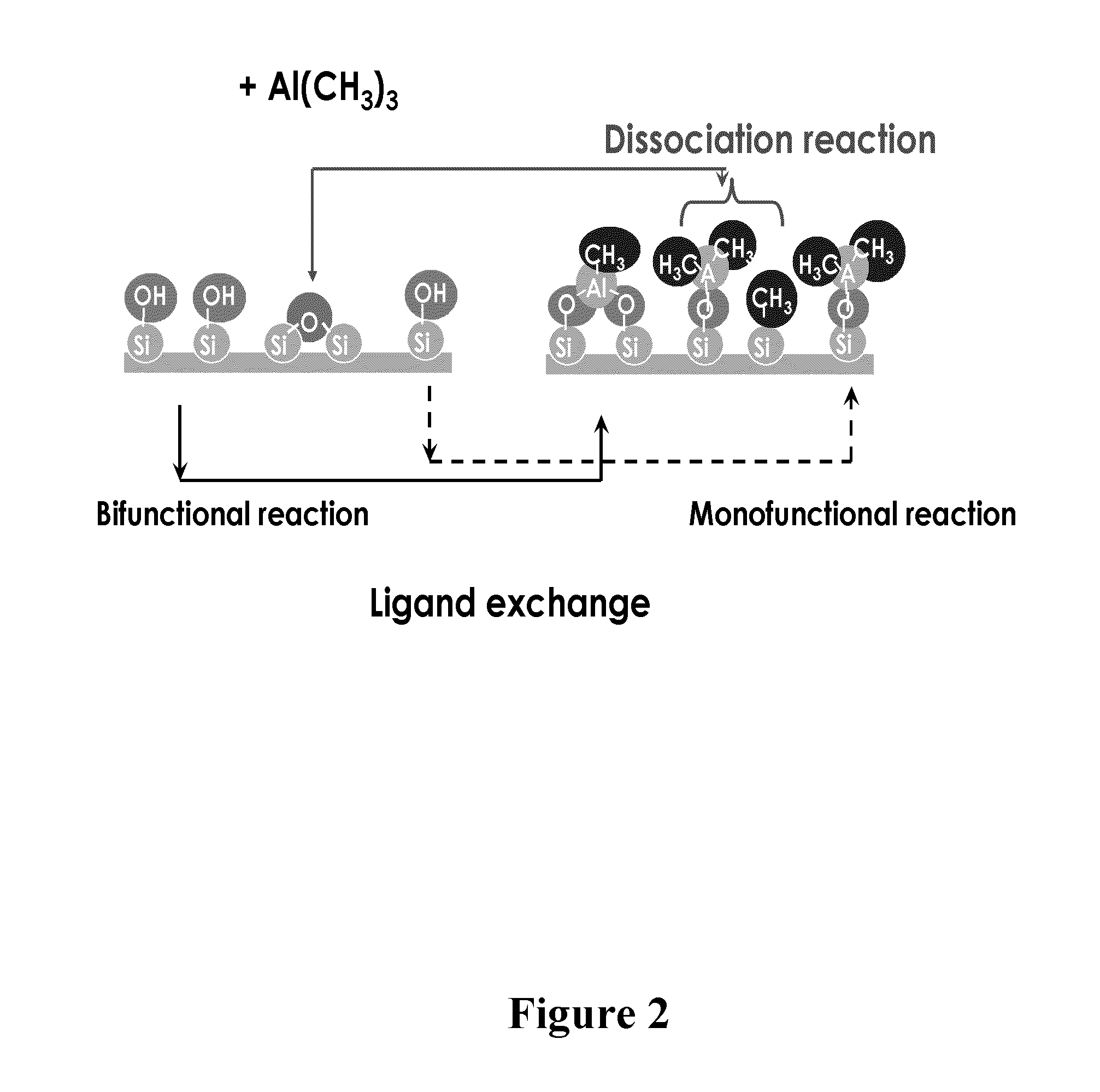
[0085]A series of experiments were performed to deposit silicon dioxide using TPS as a silicon precursor and TMA as a catalyst on a hydrophobic surface. A substrate comprising a low-k material (ASM Japan ELK 2.3) with a hydrophobic surface was contacted with TMA, followed by TPS at a temperature of 150° C. A similar reaction was performed in the absence of TMA. In the absence of TMA, no silicon dioxide growth was observed on the low-k material. However, a single pulse of TMA, followed by TPS, produced silicon dioxide growth of approximately 20 nm, which can be seen in as difference in thickness in the TEM images in FIG. 4.

example 2

[0086]Silicon dioxide is deposited on a porous, low-k material using a controlled dose of TMA as a catalyst. TPS used as the silanol.

[0087]A reactor is equipped with computer-controlled pneumatic dose valves for controlled precursor deposition. Alternating exposures of TMA and TPS are used for silicon dioxide thin film deposition. The dose of TMA is predetermined such that the depth the TMA penetration into the pores is limited and essentially only reactive sites on the top-most surface of the low-k material react with the TMA.

example 3

[0088]A copper barrier layer is formed by first depositing silicon dioxide on a hydrophobic surface of a substrate comprising a low-k material. The substrate is contacted with a pulse of TMA, the excess TMA is evacuated from the reaction space and the substrate is contacted with a pulse of TPS, thereby forming a silicon dioxide layer on the hydrophobic surface. The silicon dioxide converts the hydrophobic surface to a hydrophilic surface suitable for deposition of the barrier layer by atomic layer deposition (ALD). A barrier layer is subsequently deposited on the silicon dioxide layer by ALD.


PUM

PropertyMeasurementUnit
temperatureaaaaaaaaaa
thicknessaaaaaaaaaa

Abstract

Methods for forming silicon dioxide thin films on hydrophobic surfaces are provided. For example, in some embodiments, silicon dioxide films are deposited on porous, low-k materials. The silicon dioxide films can be deposited using a catalyst and a silanol. In some embodiments, an undersaturated dose of one or more of the reactants can be used in forming a pore-sealing layer over a porous material.

Description

REFERENCE TO RELATED APPLICATIONS[0001]The present application claims priority to U.S. provisional application No. 61 / 442,625, filed Feb. 14, 2011, which is hereby incorporated by reference in its entirety.BACKGROUND OF THE INVENTION[0002]1. Field of the Invention[0003]The present application relates generally to deposition of silicon dioxide thin films on hydrophobic surfaces, such as low-k films. The silicon dioxide films may serve, for example, as pore-sealing layers on porous low-k films.[0004]2. Description of the Related Art / Background[0005]Thin films comprising silicon dioxide are used in many different applications in microelectronic devices, for example, as dielectric materials. Silicon dioxide is one of the most commonly used dielectric materials in silicon microelectronic devices. However, silicon dioxide processes for deposition on hydrophobic surfaces without destroying the hydrophobicity have been difficult to develop.[0006]In order to decrease the k-value of low k mat...

Claims


Application Information

Patent Timeline
Patent Type & Authority Applications(United States)
IPC IPC(8): C23C16/40
CPCC23C16/402C23C16/45523H01L21/76831H01L21/0228H01L21/02164
Inventor HAUKKA, SUVITUOMINEN, MARKO
Owner ASM IP HLDG BV
Why Eureka
Try Eureka