UV curing of low-k porous dielectrics

a dielectric and porous technology, applied in the field of uv curing of low-k porous dielectric layers, can solve problems such as processing damag

Inactive Publication Date: 2007-07-12
TAIWAN SEMICON MFG CO LTD
View PDF17 Cites 57 Cited by
  • Summary
  • Abstract
  • Description
  • Claims
  • Application Information

AI Technical Summary

Benefits of technology

[0008] These and other problems are generally solved or circumvented, and technical advantages are generally achieved, by preferred embodiments of the present invention comprising a method for formation of a porous, low-k dielectric.

Problems solved by technology

The damage may include processing damage such as dangling bonds or silanol formation.

Method used


Image

  • UV curing of low-k porous dielectrics
  • UV curing of low-k porous dielectrics
  • UV curing of low-k porous dielectrics

Examples


Embodiment Construction

[0019] The operation and fabrication of the presently preferred embodiments are discussed in detail below. However, the embodiments and examples described herein are not the only applications or uses contemplated for the invention. The specific embodiments discussed are merely illustrative of specific ways to make and use the invention, and do not limit the scope of the invention or the appended claims.

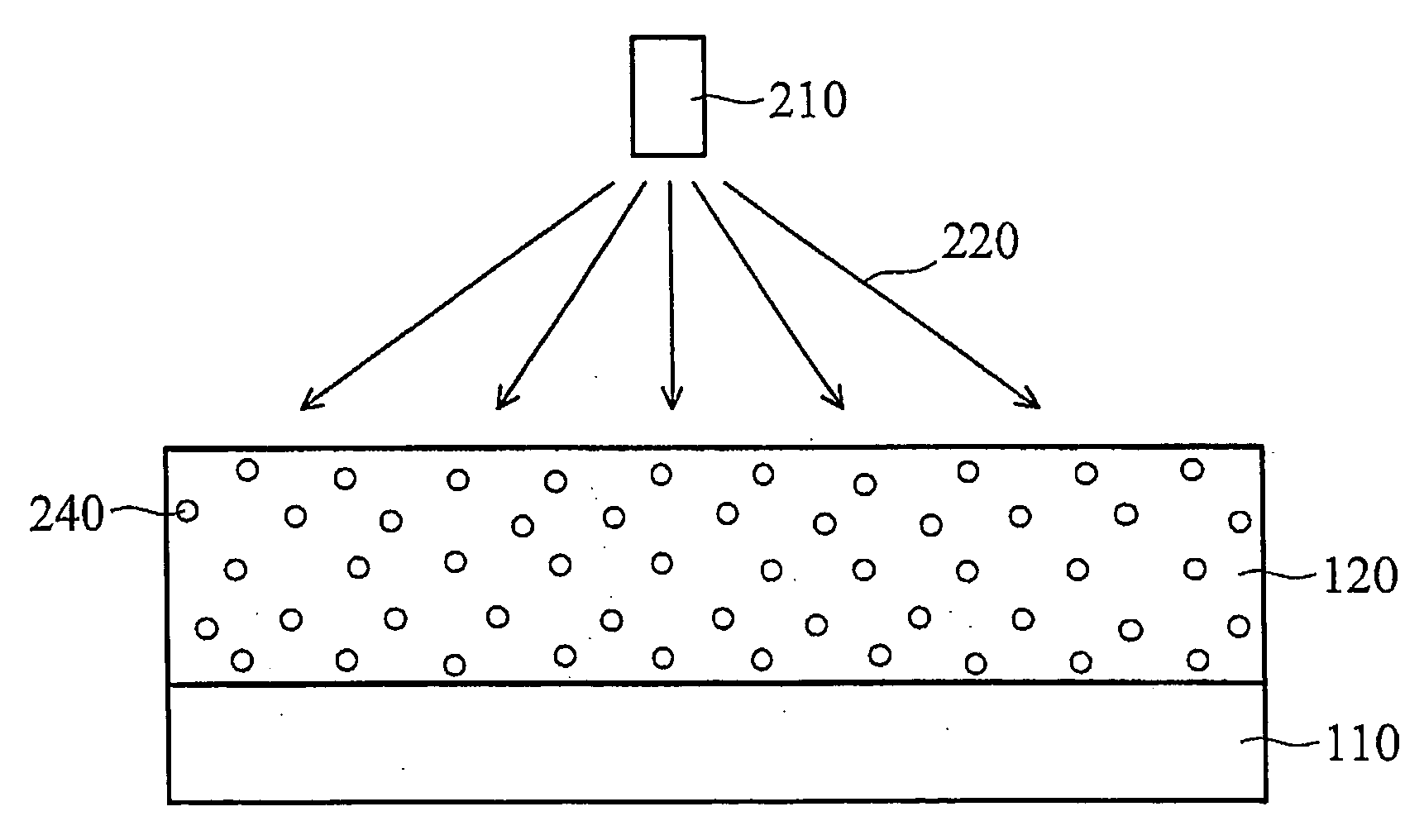
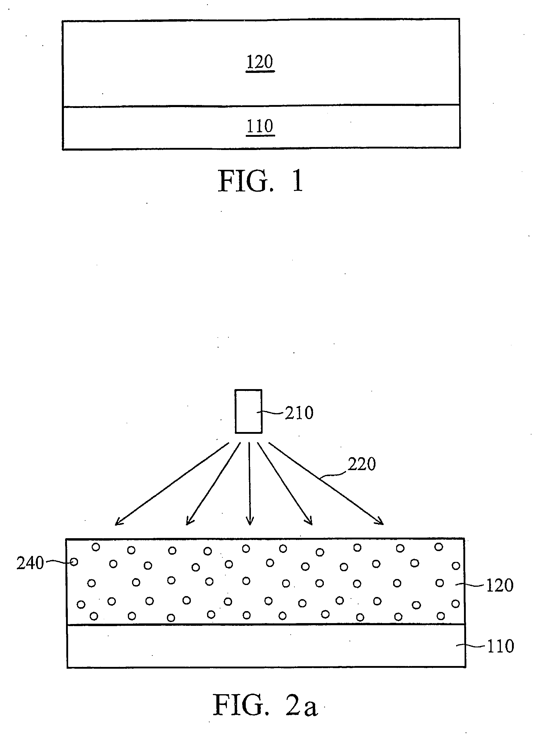
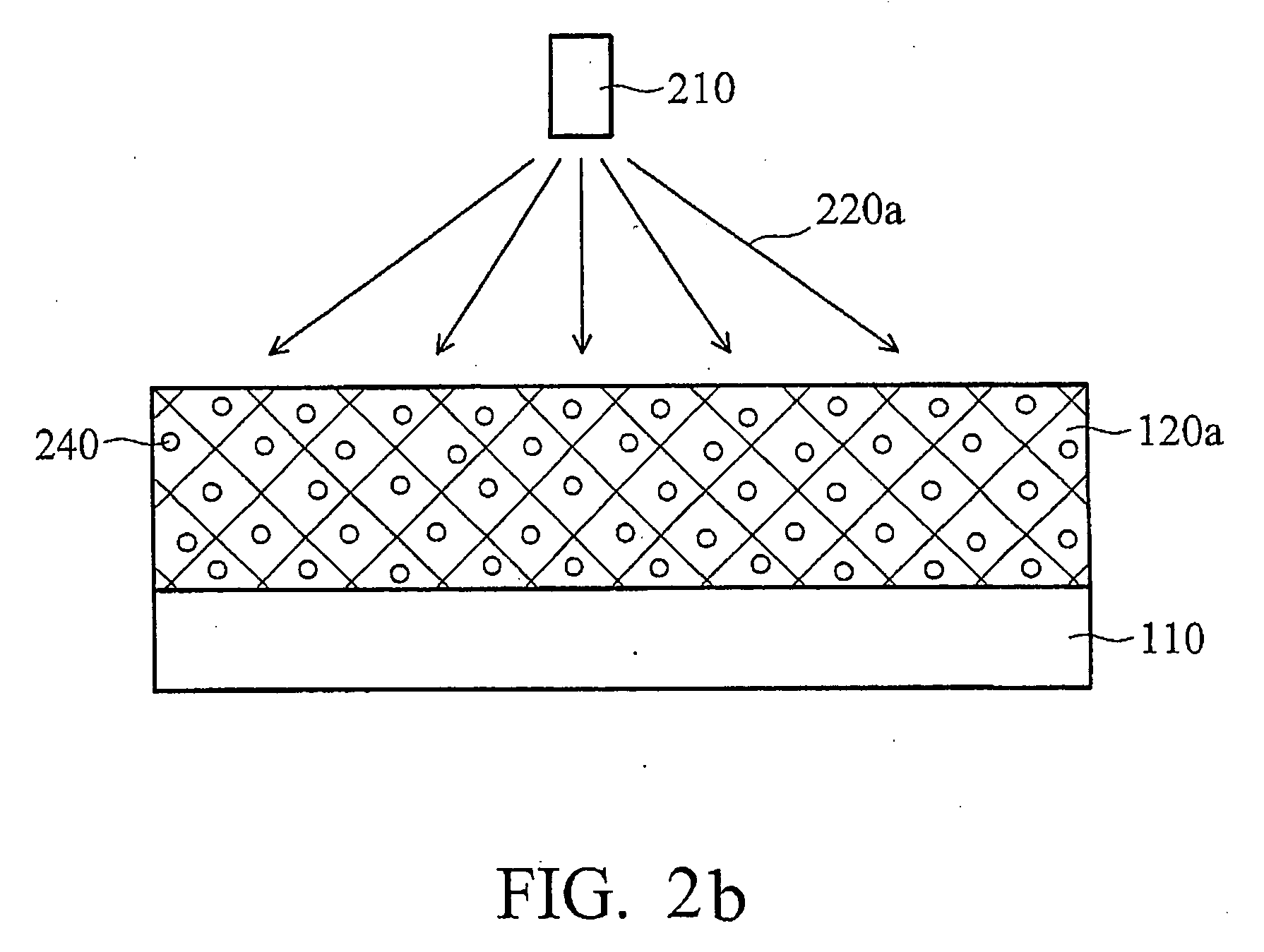
[0020] This invention relates generally to semiconductor device fabrication and more specifically to porous, low-k dielectric formation by degradation of a porogen. Referring now to FIG. 1, there is shown a typical substrate 110 used in the manufacture of semiconductor devices. The substrate 110 may comprise bulk silicon, doped or undoped, or an active layer of a silicon on insulator (SOI) substrate. Generally, an SOI substrate comprises a layer of a semiconductor material such as silicon, germanium, silicon germanium, silicon on insulator (SOI), silicon germanium on insulator (SGOI)...


PUM

PropertyMeasurementUnit
wavelengthaaaaaaaaaa
dielectric constantaaaaaaaaaa

Abstract

A method of manufacturing a semiconductor device having a low-k dielectric layer is provided. An embodiment comprises forming a dielectric layer on a substrate, wherein the layer comprises a pore generating material dispersed in an uncured matrix. A second step comprises forming pores in the uncured matrix by irradiating the layer with radiation having a first wavelength. After pore forming, a third step comprises cross-linking the dielectric by irradiating it at a second wavelength, the second being less than the first. In an embodiment, the irradiating wavelengths comprise ultra-violet radiation. Embodiments may further include repairing processing damage wherein the damage includes dangling bonds or silanol formation. The repairing includes annealing in a carbon-containing ambient such as C2H4, C3H6, or hexamethyldisilazane (HMDS).

Description

TECHNICAL FIELD [0001] This invention relates generally to semiconductor device fabrication and more particularly to a method for forming porous, low-k dielectric layers. BACKGROUND [0002] As the density of semiconductor devices increases and the size of circuit elements becomes smaller, the resistance capacitance (RC) delay time increasingly dominates the circuit performance. To reduce the RC delay, there is a desire to switch from conventional dielectrics to low-k dielectrics. These materials are particularly usefull as intermetal dielectrics, IMDs, and as interlayer dielectrics, ILDs. However, low-k materials present problems during processing, especially during the processing of the conductive material used to make interconnects. [0003] The conductive material is typically patterned and etched using high-energy plasma etch processes. In other process schemes, the low-k material is patterned through the application and patterning of photoresist. The low-k material is etched throu...

Claims


Application Information

Patent Timeline
Patent Type & Authority Applications(United States)
IPC IPC(8): H01L21/4763H01L21/469
CPCH01L21/7682H01L21/76826H01L21/76825H01L2221/1047
Inventor CHEN, I-IBAO, TIEN-ICHENG, SHWANG-MINGYU, CHEN-HUA
Owner TAIWAN SEMICON MFG CO LTD
Why Eureka
Try Eureka