

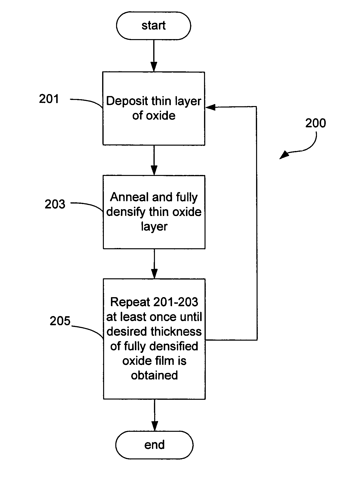
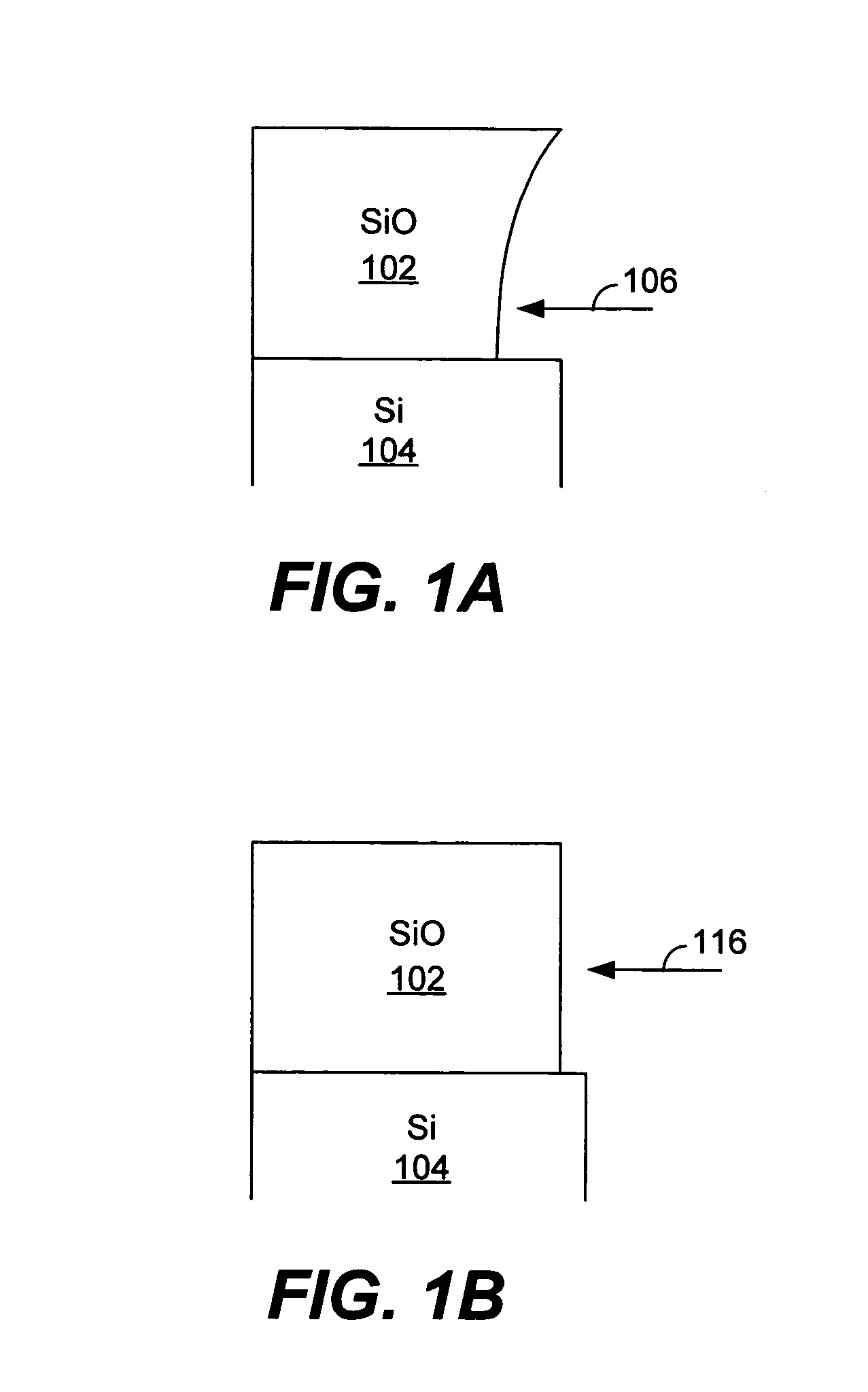
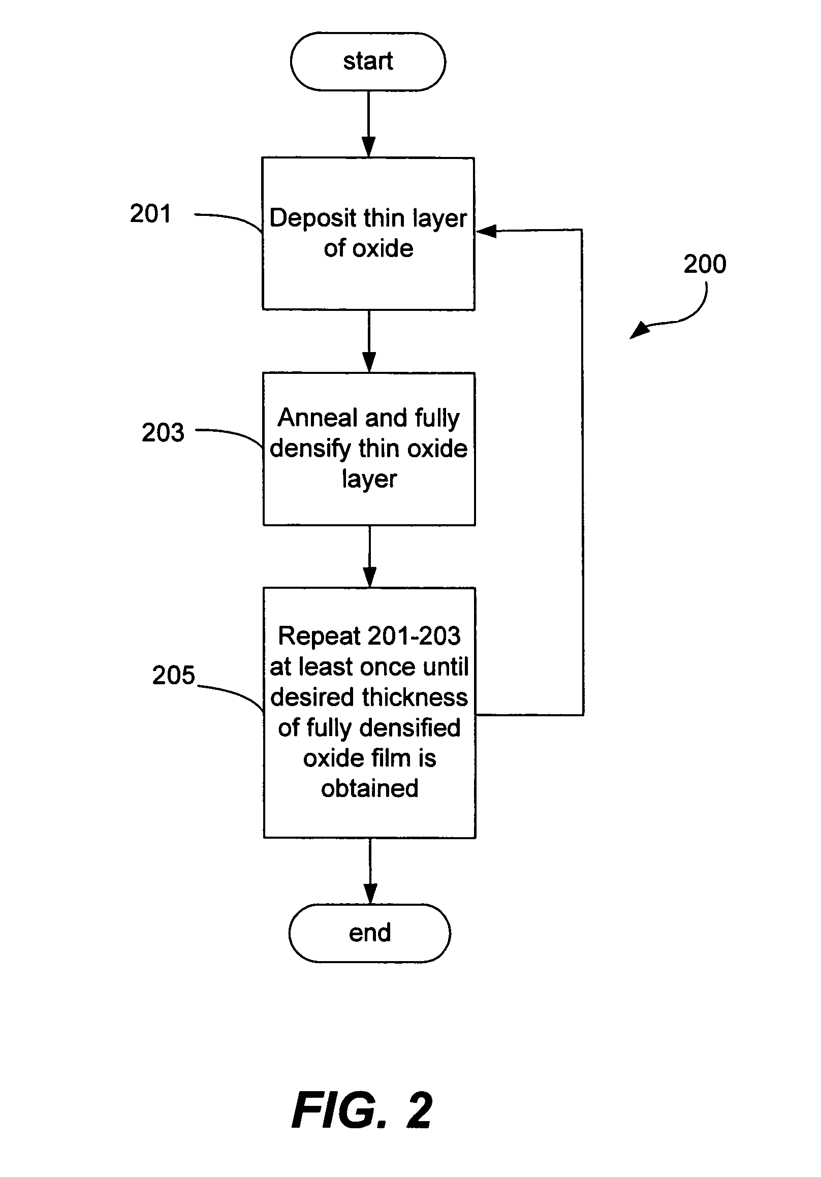
Sequential deposition/anneal film densification method
a technology of anneal film and density, applied in the field of dielectric film formation, can solve the problems of reducing budget, void-free filling of high aspect ratio space (ar>3.0:1), and shrinking dimensions, and achieve the effect of maintaining film properties
- Summary
- Abstract
- Description
- Claims
- Application Information
AI Technical Summary
Benefits of technology
Problems solved by technology
Method used
Image

Examples
example
[0078]The following example provides details relating to performance advantages of the present invention. It should be understood the following is representative only, and that the invention is not limited by the detail set forth in this example.
[0079]Annealing Efficiency
[0080]FIG. 7 shows the effect of film thickness on the efficiency of the densification (annealing) process. SiO2 films were deposited by RVD using a silicon precursor partial pressure below 10 Torr and a temperature of 230° C. Films were annealed by RTP at the temperatures indicated for at least 5 minutes at ambient pressure in a mixture of 30% steam and 70% N2. The films' wet etch rate, which is a measure of film density, was measured at the top and at the bottom of the stack. For the 5000 Å films, the difference is in the order of 40%, while for films 2000 Å thick the wet etch rate measurements were within 12% at temperatures above 700° C. This result indicates that the thinner films were more efficiently and unif...
PUM
| Property | Measurement | Unit |
|---|---|---|
| temperature | aaaaa | aaaaa |
| temperature | aaaaa | aaaaa |
| partial pressure | aaaaa | aaaaa |
Abstract
Description
Claims
Application Information