

Manufacturing method of semiconductor device
a manufacturing method and semiconductor technology, applied in the direction of semiconductor devices, basic electric elements, electrical appliances, etc., can solve the problems of deterioration of transistor characteristics such as mobility, and achieve the effect of suppressing the growth of interface silicon oxide and reducing oxygen deficiency
- Summary
- Abstract
- Description
- Claims
- Application Information
AI Technical Summary
Benefits of technology
Problems solved by technology
Method used
Image

Examples
first embodiment
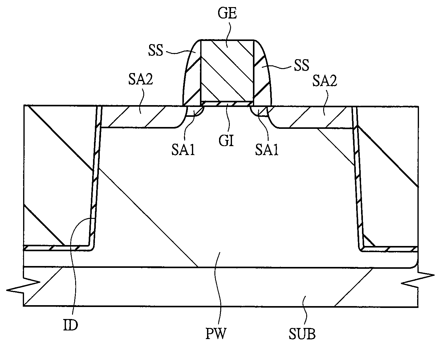
[0033]In the first embodiment, the present invention is applied to a manufacturing method of an n channel MIS transistor, which will be described with reference to FIG. 1 to FIG. 9. FIG. 1 to FIG. 9 are cross-sectional views schematically showing a semiconductor device in a manufacturing process, in which FIG. 2 to FIG. 6 show a principal part of the semiconductor device in an enlarged manner. Note that a p channel MIS transistor has an opposite polarity to that of an n channel MIS transistor, and the present invention can also be applied to a manufacturing method of a p channel MIS transistor.
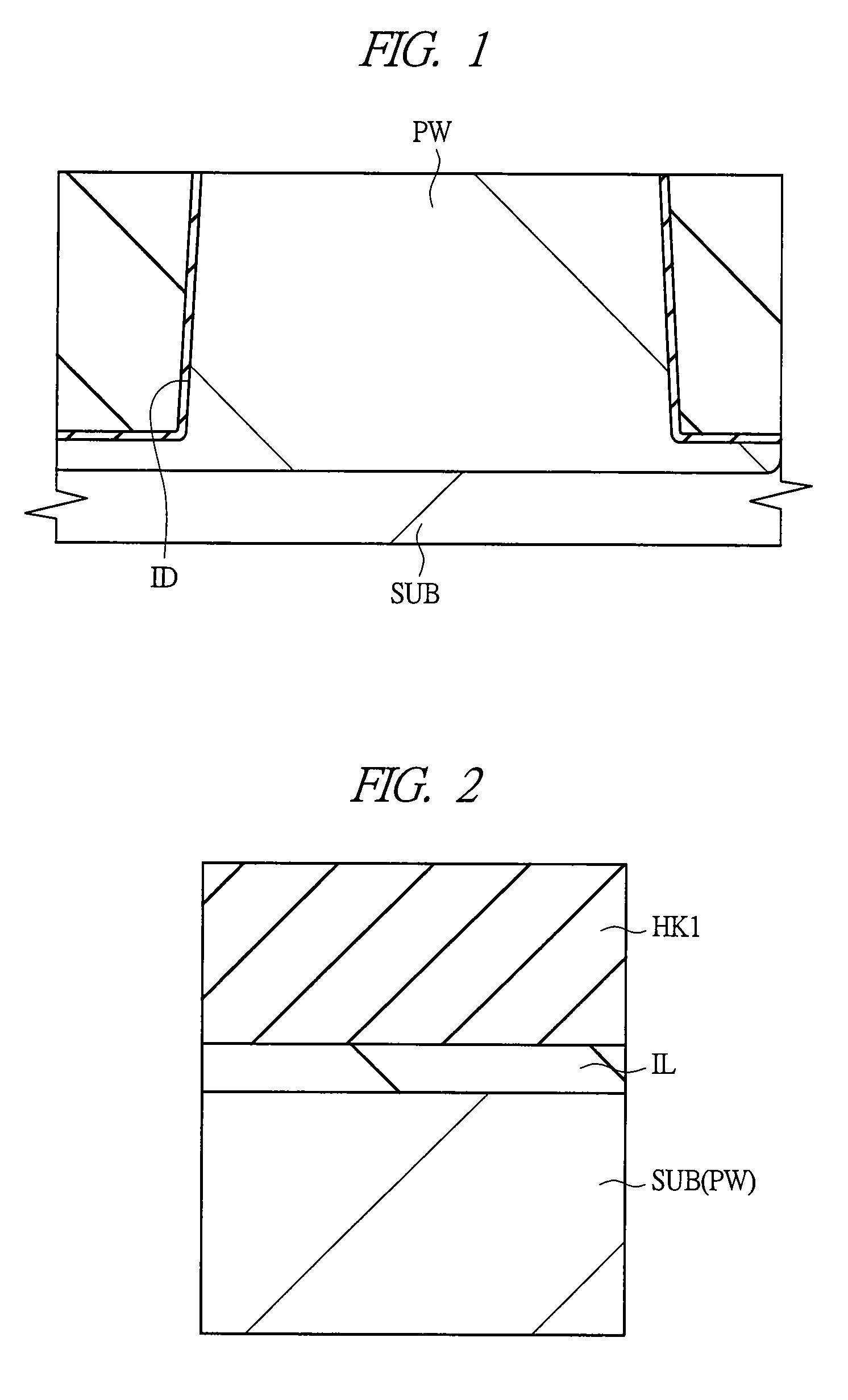
[0034]As shown in FIG. 1, element isolation trenches ID are first formed in a main surface (element formation surface) of a semiconductor substrate (hereinafter, referred to as substrate) SUB made of, for example, p type single crystal silicon by the well-known STI (Shallow Trench Isolation) technique. Next, after boron is ion-implanted in an n channel MIS transistor formation region of the su...
second embodiment
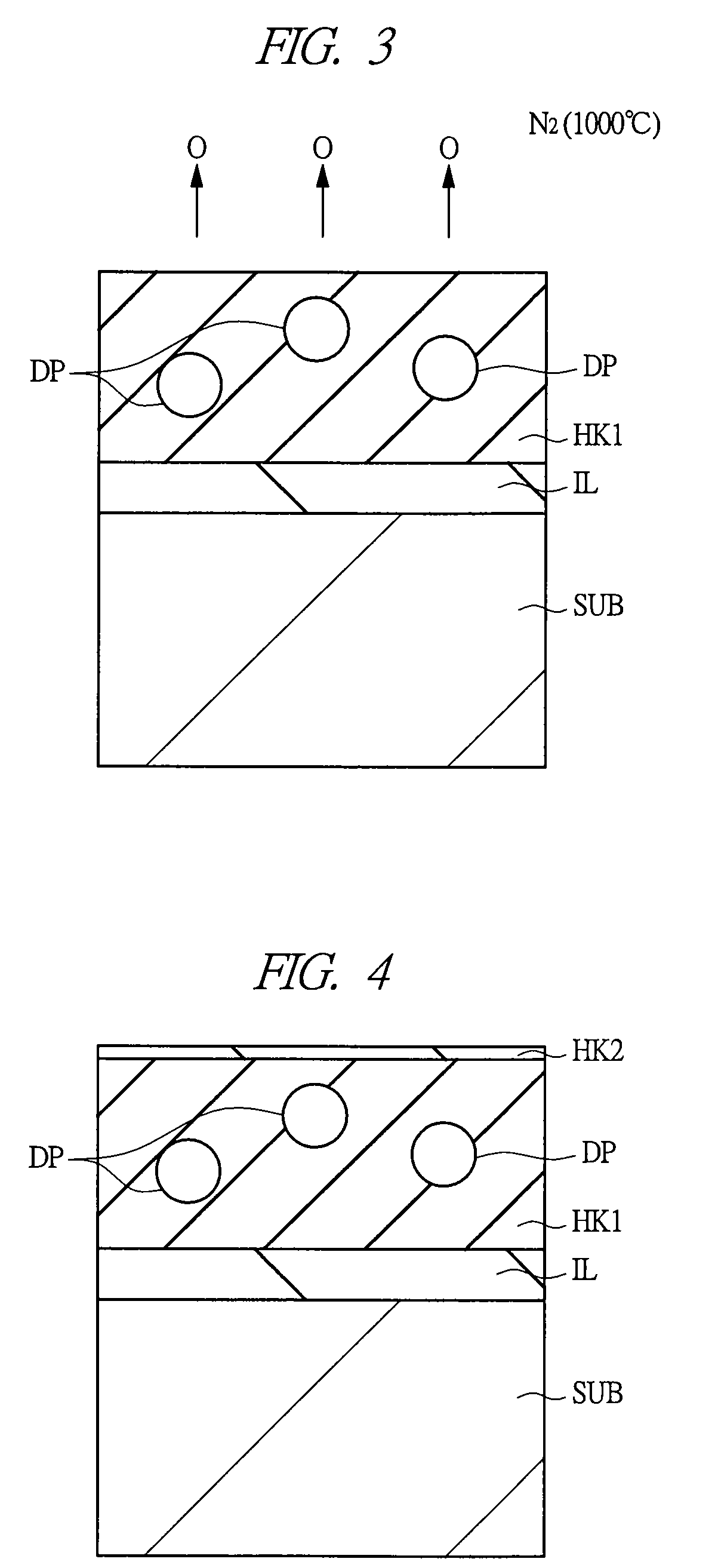
[0063]Although the case where hafnium-based oxide deposited by the ALD is used in the step of forming the oxygen supplying layer has been described in the first embodiment, the case where aluminum oxide (Al2O3) deposited by the ALD or tantalum oxide (Ta2O5) deposited by the ALD is applied to form the oxygen supplying layer will be described in the second embodiment. Note that the other steps in the second embodiment are similar to those in the first embodiment.
[0064]As described in the first embodiment, the oxygen supplying layer HK2 functions to supply oxygen to the high dielectric layer HK1 in the oxygen supplying annealing in order to supplement oxygen lost in the high dielectric layer HK1. Therefore, an oxygen supplying layer which has an oxygen concentration (oxygen proportion) higher than that in the high dielectric layer HK1 just after the densification annealing in which the oxygen deficiency has occurred can be used as the oxygen supplying layer HK2. Accordingly, the oxygen...
PUM
 Abstract
Description
Claims
Application Information