Atomic layer deposition of high-k metal oxides

a metal oxide and atomic layer technology, applied in chemical vapor deposition coatings, coatings, solid-state devices, etc., can solve the problems of electron mobility degradation in mosfet performance, leakage and reliability deficiencies of conventional gate dielectrics, and the thinness of insulators, so as to achieve superior thermal stability and less interfacial silicon dioxide growth

Inactive Publication Date: 2006-11-16
AVIZA TECHNOLOGY INC +1
View PDF9 Cites 405 Cited by
  • Summary
  • Abstract
  • Description
  • Claims
  • Application Information

AI Technical Summary

Benefits of technology

[0009] The invention provides ALD processes for forming high k Group 4 metal oxide films, including hafnium oxide (HfO2), zirconium oxide (ZrO2), and titanium oxide (TiO2), to replace silicon dioxide in g...

Problems solved by technology

Such insulators are now as thin as 20 Å. However, conventional gate dielectrics suffer from leakage and reliability deficiencies as the thickness decreases below 20 Å.
However, charge trapping related to Vt (threshold voltage) instability, and electron mobility degradation in MOSFET performance are concerns.
In addition, prior art deposition techniques, such as chemical vapor deposition (CVD), are increasingly unable to meet the requirements of advanced thin films.
While CVD processes can be tailored to provide conformal films with improved step coverage, CVD processes often requi...

Method used


Image

  • Atomic layer deposition of high-k metal oxides
  • Atomic layer deposition of high-k metal oxides
  • Atomic layer deposition of high-k metal oxides

Examples


Embodiment Construction

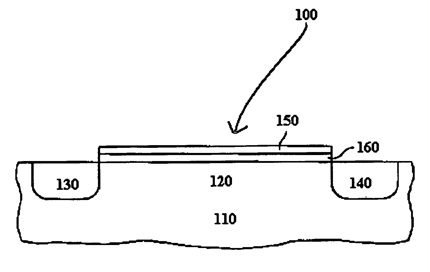
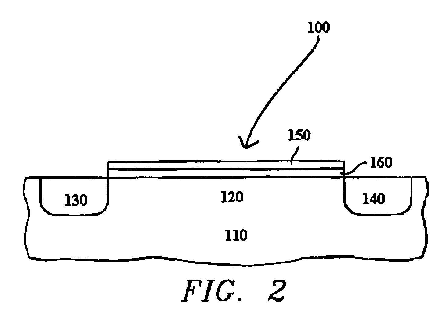
[0018] The invention provides ALD processes for forming high k Group 4 metal oxide films to replace silicon dioxide in gate and / or capacitor dielectric applications. Such metal oxides include hafnium oxide (HfO2), zirconium oxide (ZrO2), and titanium oxide (TiO2). The most preferred metal oxide is hafnium oxide.

[0019] Prior to starting the pulse cycle, a substrate, generally a silicon wafer, is placed into a reaction chamber, often through a valve located at one end of the chamber. Preferably, the silicon wafer has been cleaned with hydrogen fluoride to remove native silicon dioxide.

[0020] The substrate sits on a heatable wafer holder that supports and heats the substrate to the desired reaction temperature. Once the substrate is properly positioned, the pulse cycle can begin.

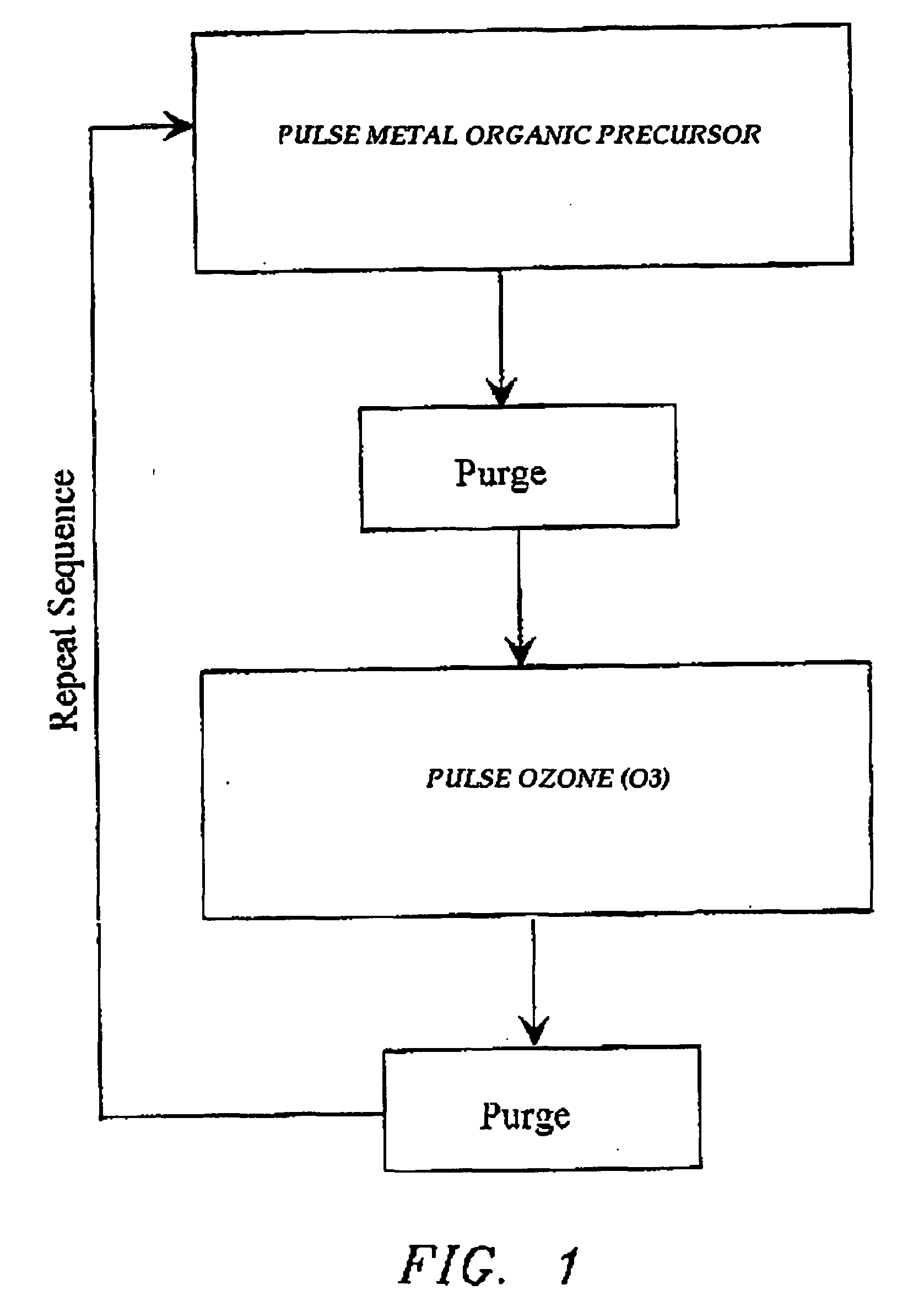
[0021] Generally, prior to the first pulse in the pulse cycle, the wafer is heated to a temperature ranging from about 100° C. to about 500° C., and preferably ranging from about 200° C. to about 400° C. Thi...


PUM

PropertyMeasurementUnit
Dielectric polarization enthalpyaaaaaaaaaa

Abstract

The present invention relates to the atomic layer deposition (“ALD”) of high k dielectric layers of metal oxides containing Group 4 metals, including hafnium oxide, zirconium oxide, and titanium oxide. More particularly, the present invention relates to the ALD formation of Group 4 metal oxide films using an metal alkyl amide as a metal organic precursor and ozone as a co-reactant.

Description

CROSS-REFERENCE TO RELATED APPLICATIONS [0001] This application is related to, and claims priority to, U.S. Provisional Patent Application No. 60 / 404,372, entitled Atomic Layer Deposition of High-k Metal Oxides for Gate and Capacitor Dielectrics, filed Aug. 18, 2002, the entire disclosure of which is hereby incorporated by reference.FIELD OF THE INVENTION [0002] The present invention relates to the atomic layer deposition (“ALD”) of high k dielectric films of metal oxide that contain Group 4 metals (Group 4 being the new periodic table notation which corresponds to Group IVA in the previous IUPAC form and Group IVB in the CAS version), including hafnium oxide (HfO2), zirconium oxide (Z1O2) and titanium oxide (TiO2), for gate and / or capacitor applications. More particularly, the present invention relates to the ALD formation of Group 4 metal oxide films using a metal alkyl amide and ozone. BACKGROUND OF THE INVENTION [0003] The speed and functionality of computers doubles every year,...

Claims


Application Information

Patent Timeline
IPC IPC(8): H01L21/8238C23C16/40H01L27/04C23C16/44C23C16/455H01LH01L21/20H01L21/31H01L21/314H01L21/316H01L21/822H01L29/78
CPCC23C16/405C23C16/45531C23C16/45553H01L21/28194H01L29/517H01L21/31604H01L21/31641H01L21/31645H01L21/3141H01L21/02205H01L21/02189H01L21/02181H01L21/0228H01L21/02186H01L21/20
Inventor LEE, SANG-INSENZAKI, YOSHIHIDELEE, SANG-KYOO
Owner AVIZA TECHNOLOGY INC
Why Eureka
Try Eureka