Heat treatment jig for semiconductor silicon substrate

a heat treatment jig and semiconductor silicon technology, applied in the direction of charging supports, lighting and heating apparatus, furniture, etc., can solve the problems of low-density grown-in defects, affecting device characteristics, and progressively lowering temperatures and higher degrees of integration

Active Publication Date: 2007-01-16
SUMITOMO MITSUBISHI SILICON CORP
View PDF14 Cites 347 Cited by
  • Summary
  • Abstract
  • Description
  • Claims
  • Application Information

AI Technical Summary

Problems solved by technology

Furthermore, in device processes, there has been a trend toward progressively lower temperatures and higher degrees of integration, and it has become clear that low-density grown-in defects formed during crystal growth, which were not a problem in the past, have begun to affect device characteristics.
In the case of the abovementioned respective heat treatment of hydrogen annealing or argon annealing, a high-temperature heat treatment at a temperature of 1100° C. or higher is necessary, so that the problem of crystal defects, for example, such as slipping and dislocations, arise as a result of the stress caused by the weight of the wafer itself in the heat treatment process as the diameter of the wafer being treated increases.
Furthermore, in the case of the abovementioned horseshoe type heat treatment jig shown in FIG. 1A, which has a structure that allows the passage of the tweezers for transfering the silicon substrate, the deflection of the heat treatment jig itself becomes noticeable, so that the problem of conspicuous slipping arises.
In actuality, however, in the holding of the substrates by contact with the ring as a whole, the problem of the local occurrence of slipping and dislocations in the regions of contact with the ring part of the jig occurs in the silicon substrates following heat treatment, as a result of problems in the machining precision of the jig and other jig formation problems.
Furthermore, since such jigs have a complete ring structure, the silicon substrates cannot be loaded and unloaded using an automated transfer method that employs the abovementioned tweezers, so that an extensive modification of the heat treatment furnace is required.
In this case, however, fine projections ranging in size from several microns to several tens of microns grow on the surface in the manufacturing stage, so that slipping occurs in the silicon wafer that contacts these regions.

Method used


Image

  • Heat treatment jig for semiconductor silicon substrate
  • Heat treatment jig for semiconductor silicon substrate
  • Heat treatment jig for semiconductor silicon substrate

Examples


embodiment 1

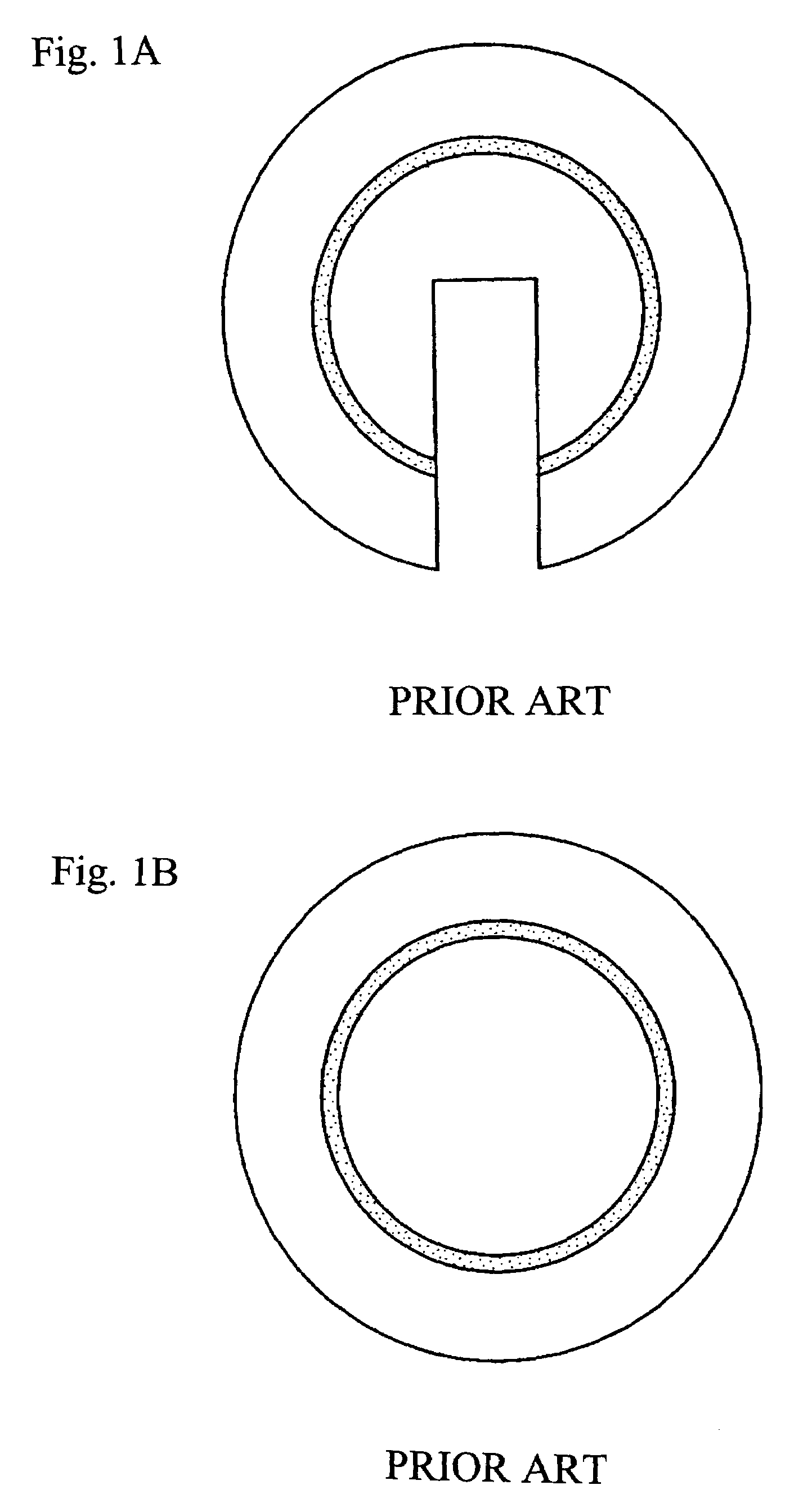
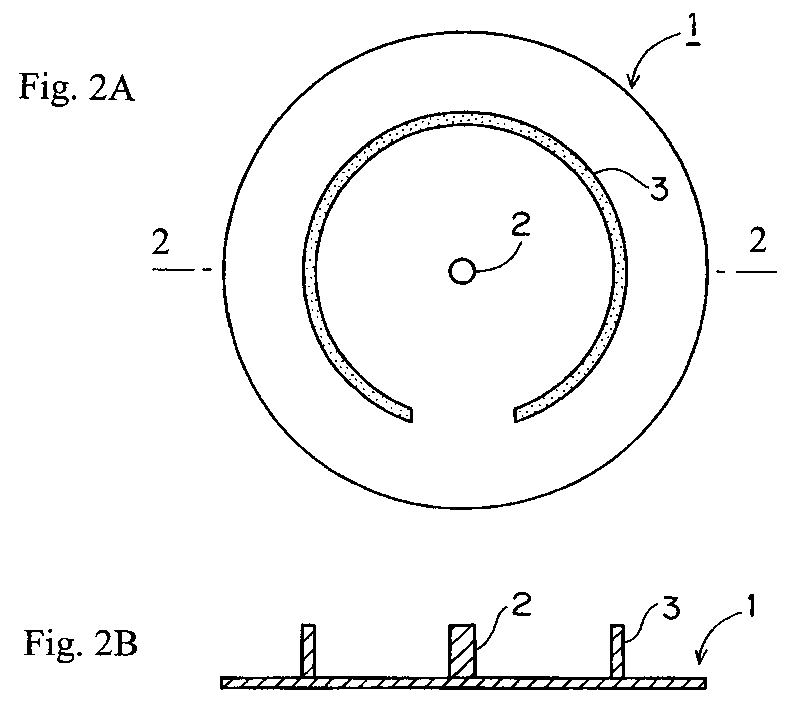
[0059]Using the silicon carbide heat treatment jig of the present invention shown in FIG. 2, in which the heights of both the circular arc part and central projecting part were set at 5 mm, and the silicon carbide heat treatment jig of the present invention shown in FIG. 3, in which the circular arc height was set at 2 mm and the height of the central projecting part was set at 5 mm, these jigs were set in a heat treatment boat beforehand, the silicon substrate was automatically transferred, and a heat treatment similar to that performed in Comparative Example 1 was performed. The transferred silicon substrate was observed using X-rays, and the conditions of slipping were checked.

embodiment 2

[0060]The heat treatment jig of Embodiment 1 of the present invention was subjected to a heat treatment for 4 hours at 1200° C. in a 100% oxygen atmosphere. Afterward, the oxidation film that was grown on the heat treatment jig was stripped away by means of an aqueous solution of hydrofluoric acid. After this operation was repeated three times, a heat treatment similar to that performed in Embodiment 1 was performed. The transferred silicon substrate was observed using X-rays, and the conditions of slipping were checked.

embodiment 3

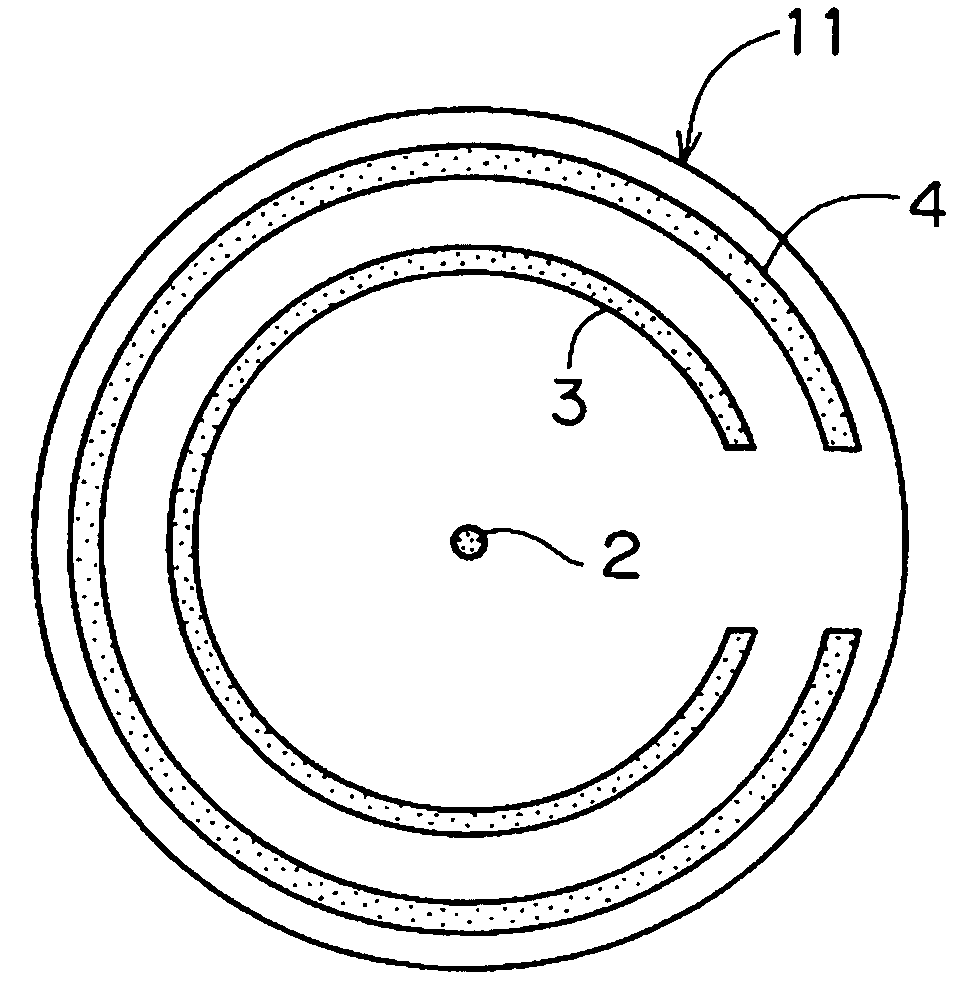
[0061]Using the silicon carbide jig of the present invention constructed as shown in FIGS. 6A and 6B, in which the heights of both the circular arc parts and the central projecting part were set at 5 mm, this jig was mounted in a heat treatment boat beforehand, the silicon substrate was automatically transferred, and a heat treatment similar to that performed in Comparative Example 1 was performed. The transferred silicon substrate was observed using X-rays, and the conditions of slipping were checked.


PUM

PropertyMeasurementUnit
thicknessaaaaaaaaaa
thicknessaaaaaaaaaa
temperatureaaaaaaaaaa

Abstract

This invention provides a heat treatment jig for semiconductor silicon substrates, which, in respective heat treatment of hydrogen annealing or argon annealing, can handle enlargement of the diameter of wafers to be treated and can also prevent slipping and dislocations that occur as a result of the stress caused by the weight of the wafer itself or the deflection of the heat treatment jig itself.

Description

FIELD OF THE INVENTION[0001]The present invention relates to an improvement of a heat treatment jig for heat treating semiconductor silicon substrates, and more particularly to a heat treatment jig for a semiconductor silicon substrate in which slipping and dislocation can be reduced by combining a central projecting part which supports the central portion of the silicon substrate, and circular-arc parts which are disposed concentrically with this central projecting part.[0002]By comprising one or more circular-arc parts on the heat treatment jig and providing a central projecting part, which is at least as high as or slightly lower than the circular-arc parts, on a position corresponding to the central portion of the silicon substrate, substrate contact at the central projecting part can be reliably achieved, and a structure, in which the stress caused by the weight of the substrate itself can be more efficiently dispersed along with a contact at the circular-arc parts, can be obta...

Claims


Application Information

Patent Timeline
Patent Type & Authority Patents(United States)
IPC IPC(8): F27D5/00H01L21/677H01L21/687
CPCF27D5/0037H01L21/6875H01L21/67748
Inventor ADACHI, NAOSHI
Owner SUMITOMO MITSUBISHI SILICON CORP
Why Eureka
Try Eureka