Low 1c screw dislocation 3 inch silicon carbide wafer

a silicon carbide wafer and screw technology, applied in the direction of polycrystalline material growth, crystal growth process, transportation and packaging, etc., can solve the problems of limiting the performance characteristics of devices made on the substrate, difficult to eliminate relatively high defect concentrations, and constant reduction of structural defects in silicon carbide bulk crystals. achieve the effect of high quality

Active Publication Date: 2008-01-01
CREE INC
View PDF25 Cites 162 Cited by
  • Summary
  • Abstract
  • Description
  • Claims
  • Application Information

AI Technical Summary

Problems solved by technology

Although the density of structural defects in silicon carbide bulk crystals has been continually reduced in recent years, relatively high defect concentrations still appear and have been found to be difficult to eliminate, e.g. Nakamura et al., “Ultrahigh quality silicon carbide single crystals,”Nature, Vol. 430, Aug. 26, 2004, page 1009.
These defects can cause significant problems in limiting the performance characteristics of devices made on the substrates, or in some cases can preclude useful devices altogether.
Current seeded sublimation techniques for the production of large bulk single crystals of silicon carbide typically result in a higher than desired concentration of defects on the growing surface of the silicon carbide crystal.
Higher concentrations of defects can cause significant problems in limiting the performance characteristics of devices made on the crystals, or substrates resulting from the crystals.
Thus, the commercial availability of 50 mm (2″) and 75 mm (3″) SiC wafers lags behind these other materials and to some extent limits the adoption and use of SiC in a wider range of devices and applications.
Screw dislocations, particularly 1 c screw dislocations, are common defects that develop or propagate during the production of SiC crystals.
Other surface defects include threading dislocations, hexagonal voids, and micropipes.
If these defects remain in the SiC crystal, then resulting devices grown on the crystal may incorporate these defects.
The presence of a large number of screw dislocations can also lead to the presence of other defects, such as micropipes and hexagonal voids.
The presence of surface defects in bulk single crystals of SiC may also interfere with single-polytype crystal growth.
The 150 available polytypes of SiC raise a particular difficulty.
Maintaining the desired polytype identity throughout the crystal is only one difficulty in growing SiC crystals of large sizes in a seeded sublimation system.
When surface defects are present, there is not enough polytype information on the crystal surface for depositing layers to maintain the desired polytype.
Polytype changes on the surface of the growing crystal result in the formation of even more surface defects.
Recent research indicates that problems in the bulk crystals produced in a seeded sublimation technique can originate with the seed itself and the manner in which it is physically handled; e.g., Sanchez et al Formation Of Thermal Decomposition Cavities In Physical Vapor Transport Of Silicon Carbide, Journal of Electronic Materials, Volume 29, No. 3, page 347 (2000).

Method used


Image

  • Low 1c screw dislocation 3 inch silicon carbide wafer
  • Low 1c screw dislocation 3 inch silicon carbide wafer
  • Low 1c screw dislocation 3 inch silicon carbide wafer

Examples


Embodiment Construction

[0026]The present invention relates to high quality silicon carbide wafers. In particular, the present invention incorporates several techniques for improving the growth of such wafers using seeded sublimation.

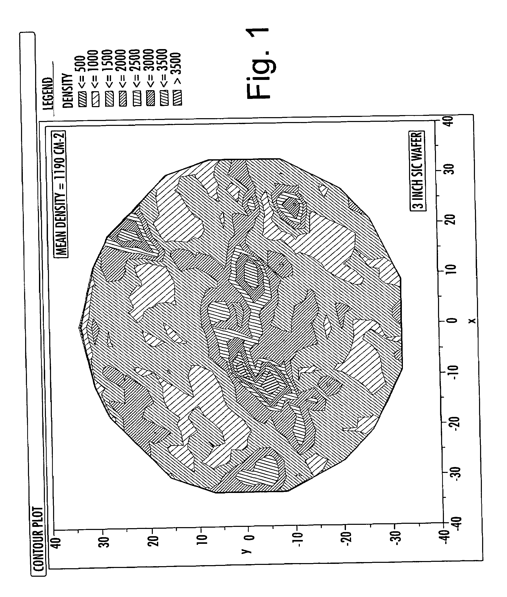
[0027]In one aspect, the present invention is a high quality single crystal wafer of SiC having a diameter of at least about 3 inches and a 1 c screw dislocation density less than about 2000 cm−2, more preferably less than about 1500 cm−2, and most preferably less than about 1000 cm−2. The polytype of the single crystal SiC is preferably 3C, 4H, 6H, or 15R.

[0028]In considering the proportional dimensions of the diameter and thickness of the seed crystal, whether expressed as a percentage, a fraction, or a ratio, it will be understood that in the context of the improvements provided by the invention, these proportions have their inventive meaning in the context of the larger-diameter seed crystals that are described herein.

[0029]Accordingly, in certain embodiments the invention...


PUM

PropertyMeasurementUnit
diameteraaaaaaaaaa
temperatureaaaaaaaaaa
temperaturesaaaaaaaaaa

Abstract

A high quality single crystal wafer of SiC is disclosed having a diameter of at least about 3 inches and a 1 c screw dislocation density of less than about 2000 cm−2.

Description

STATEMENT OF GOVERNMENT INTEREST[0001]This invention was developed under Office of Naval Research / DARPA Contract No. N00014-02-C-0306. The government may have certain rights in this invention.BACKGROUND OF THE INVENTION[0002]The present invention relates to low defect silicon carbide wafers and their use as precursors for semiconductor purposes, and to seeded sublimation growth of large, high-quality silicon carbide single crystals.[0003]Silicon carbide has found use as semiconductor material for various electronic devices and purposes in recent years. Silicon carbide is especially useful due to its physical strength and high resistance to chemical attack. Silicon carbide also has excellent electronic properties, including radiation hardness, high breakdown field, a relatively wide band gap, high saturated electron drift velocity, high-temperature operation, and absorption and emission of high-energy photons in the blue, violet, and ultraviolet regions of the spectrum.[0004]Single c...

Claims


Application Information

Patent Timeline
Patent Type & Authority Patents(United States)
IPC IPC(8): C30B25/12
CPCC30B23/00H01L29/1608C30B29/36Y10T428/21
Inventor POWELL, ADRIANBRADY, MARKMUELLER, STEPHEN G.TSVETKOV, VALERI F.LEONARD, ROBERT T.
Owner CREE INC
Why Eureka
Try Eureka