GaN field-effect transistor and method of manufacturing the same

a technology of field-effect transistors and transistors, which is applied in the direction of polycrystalline material growth, chemistry apparatus and processes, crystal growth processes, etc., can solve the problems of high breakdown voltage, difficult to produce single-crystal substrates with a large diameter, and inability to form a fet-layer structur

Inactive Publication Date: 2001-11-15
FURUKAWA ELECTRIC CO LTD
View PDF0 Cites 160 Cited by
  • Summary
  • Abstract
  • Description
  • Claims
  • Application Information

AI Technical Summary

Benefits of technology

0017] It is an object of the present invention to provide a high-performance GaN FET constructed to have a GaN crystal layer structure having a portion for an FET function in which dislocation density of GaN crystals is largely decreased, thereby allowing the FET to exploit the full potential of characteristic features of GaN crystals.

Problems solved by technology

When a GaN-based material is used, differently from a case where an Si crystal, a GaAs crystal or an InP crystal is employed, it is difficult to produce a single-crystal substrate having a large diameter, which makes it impossible to form an FET-layer structure by epitaxially growing a predetermined crystal layer on a GaN single-crystal substrate.
However, due to a large lattice misfit between the buffer layer 2 and the substrate 1, the buffer layer 2 contains threading dislocations (defects) that extend generally vertically in a direction of film thickness.
(1) During operation of the FET, for example, when the FET is in its pinch-off state, the electric lines of force concentrate in a region R in the layer structure including a region R.sub.1 immediately under the gate electrode G as one of the electrodes and a region R.sub.2 adjacent to the region R.sub.1 and spreading laterally toward the drain electrode D side, particularly concentrate in the region R.sub.1. Therefore, if the GaN crystal forming the region R has a low dislocation density and hence a high quality, the region is expected to exhibit a high breakdown voltage. Actually, however, the above FET (FET as shown in FIG. 1) can undergo electrical breakdown at an extremely low field, since there exist numerous threading dislocations in the region R as well.
(2) When a bias voltage is applied to the gate electrode G so as to place the FET in an OFF state in which no current flows between the source electrode and the drain electrode thereof, a considerable amount of leak current can flow between the source electrode S and the drain electrode D.
(3) When the FET is a MESFET type having a Schottky barrier formed in a portion where the gate electrode G is formed, a reverse breakdown voltage of the gate electrode G can be lowered, or a reverse current can be increased.
(4) Further, contact resistance at respective ohmic contacts of the source electrode and the drain electrode to the layer structure 3 increases, and hence effective mobility as the property of the FET decreases, which degrades the driving power of the FET.
As described above, in the conventional GaN FET shown in FIG. 1, the threading dislocations (defects) are produced at a high dislocation density in the GaN crystals having a layer structure, at a location of the region R including the region immediately under the electrode and the region adjacent thereto, causing degradation of the quality of the GaN crystals, which prevents the FET from reaching its full potential of performance intended by the design.

Method used


Image

  • GaN field-effect transistor and method of manufacturing the same
  • GaN field-effect transistor and method of manufacturing the same
  • GaN field-effect transistor and method of manufacturing the same

Examples


example 2

[0147] Example 2

[0148] A lateral GaN FET device having a structure shown in cross section in FIG. 26 was designed as an example of the FET (2) according to the present invention.

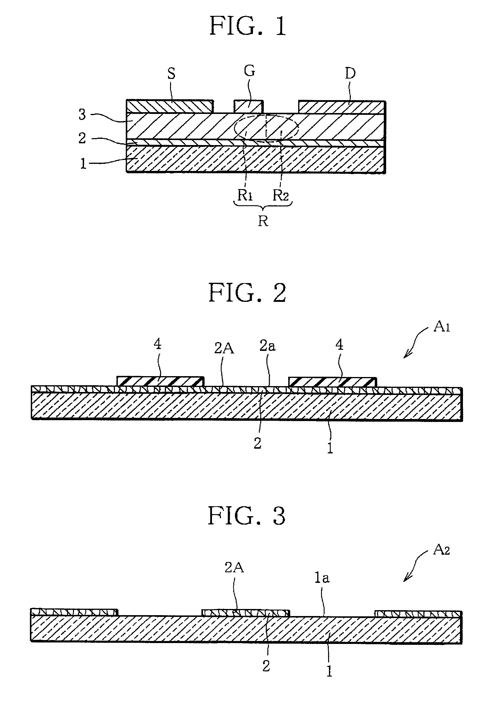
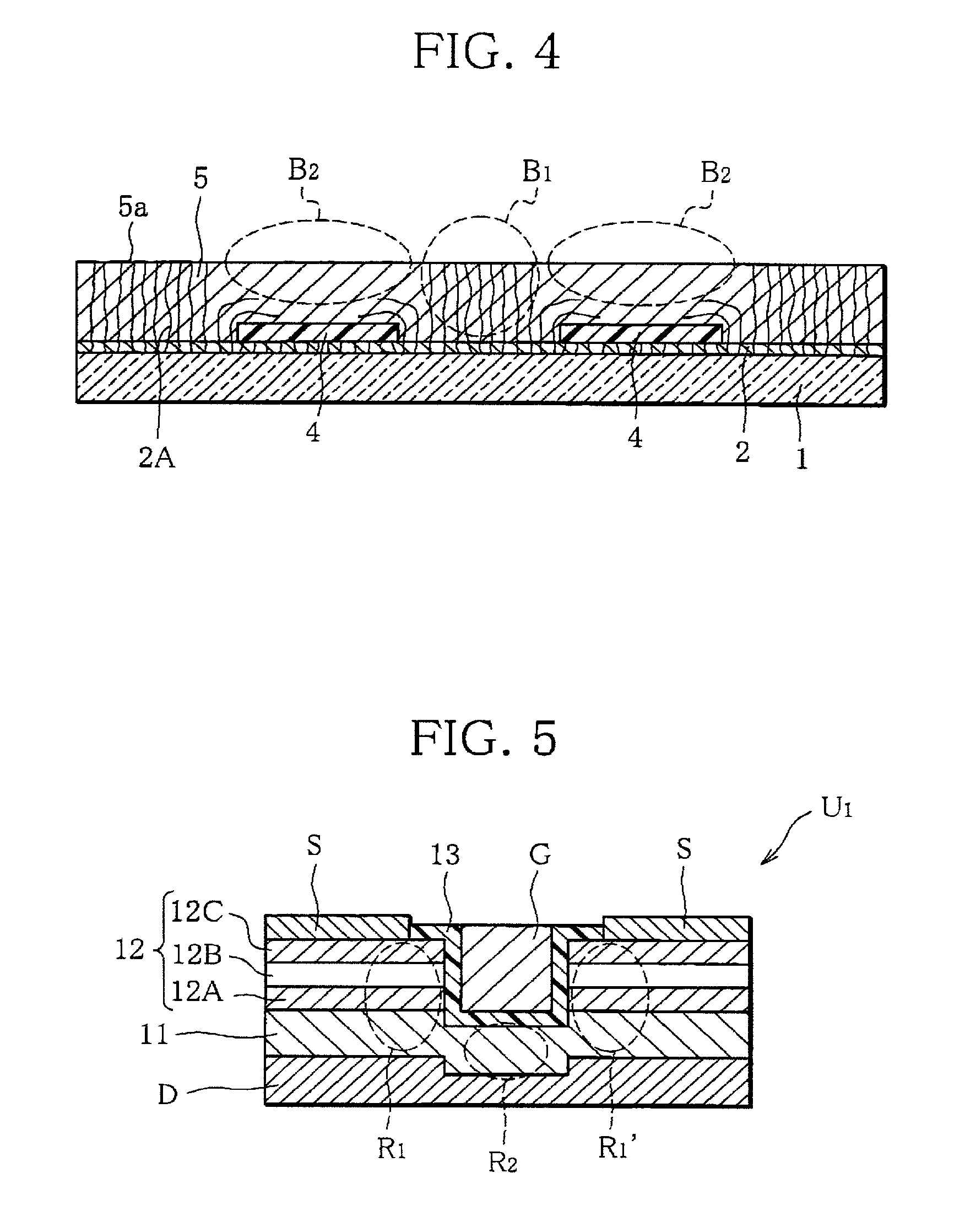
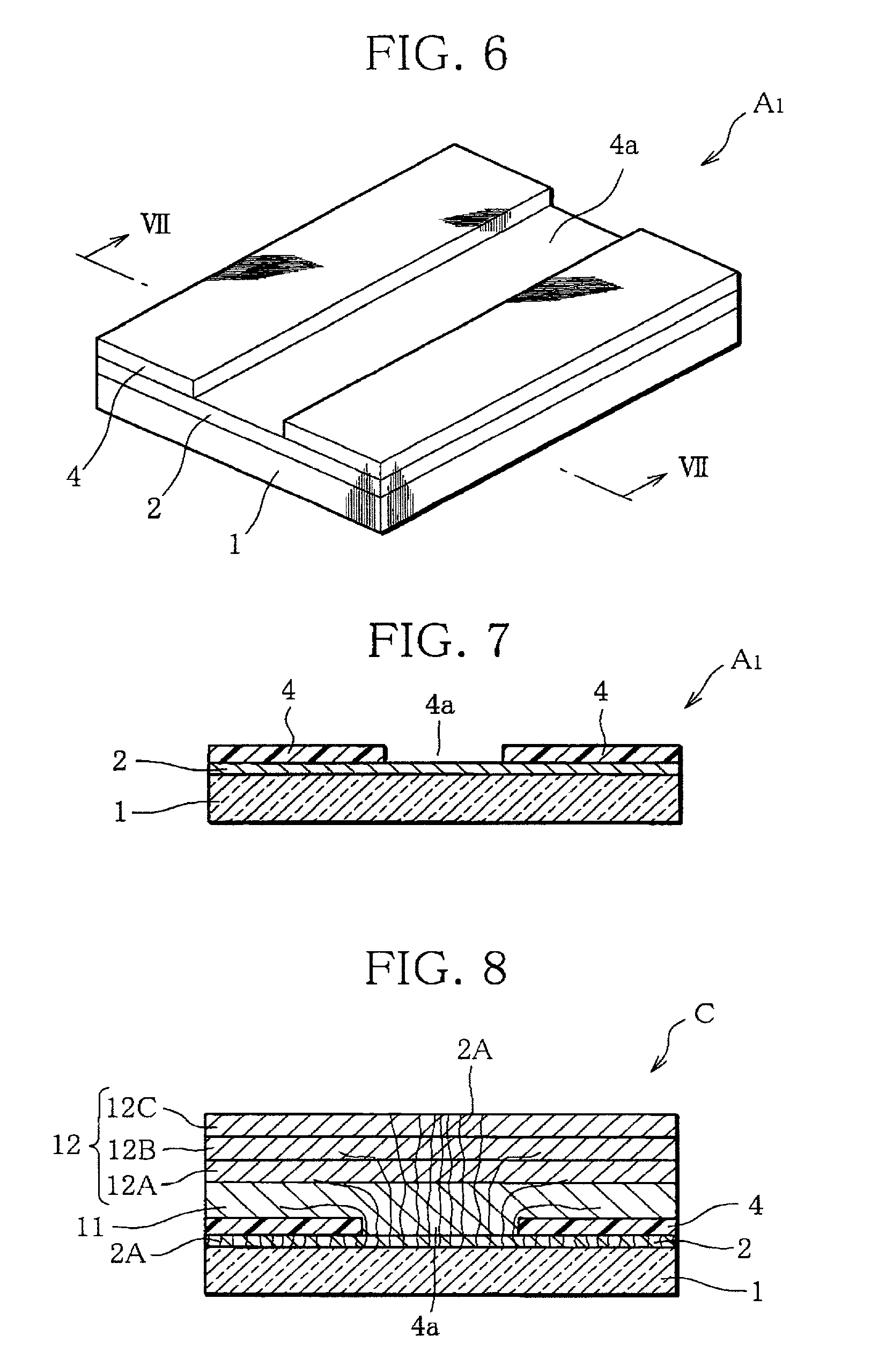
[0149] According to the designed device, a GaN crystal layer structure 15 is comprised of a high-resistance GaN crystal layer 15A formed of Mg-doped GaN, and a conductive GaN crystal layer 15B formed of Si-doped GaN. The conductive GaN crystal layer 15B is comprised of an Si-doped GaN crystal layer 15b.sub.1 serving as a channel layer and an Si-doped GaN crystal layer 15b.sub.2 serving as a contact layer for contact between source electrodes S and drain electrodes D. The space between each source electrode S and a neighboring drain electrode D is set to 3 .mu.m, and a gate electrode G having a width of 0.5 .mu.m is disposed therebetween. The whole upper surface of the device is protected by an SiO.sub.2 film 21.

[0150] Before manufacturing of the above designed device, first, a crystal-growing substrate A.sub...


PUM

PropertyMeasurementUnit
temperatureaaaaaaaaaa
widthaaaaaaaaaa
widthaaaaaaaaaa

Abstract

There are provided a GaN field effect transistor (FET) exhibiting an excellent breakdown voltage owing to the high quality of GaN crystal in a region where the electric lines of force concentrate during operation of the same, and a method of manufacturing the same. The FET has a layer structure formed of a plurality of GaN epitaxial layers. A gate electrode and a source electrode are disposed on the surface of the layer structure, and a drain electrode is disposed on the reverse surface of the same. A region of the layer structure in which the electric lines of force concentrate during operation of the FET has a reduced dislocation density compared with the other regions in the layer structure. The GaN FET is manufactured by forming, on a crystal-growing substrate having a surface formed with a plane pattern of a material other than a GaN-based material in an identical design to a plane pattern of an electrode determining the region in which the electric lines of force concentrate, a plurality of GaN epitaxial layers, one upon another, by using the epitaxial lateral overgrowth technique, thereby forming a layer structure, and then forming operational electrodes on the surface of the layer structure.

Description

[0001] 1. Field of the Invention[0002] The present invention relates to a GaN field-effect transistor and a method of manufacturing the same, and more particularly to a GaN field-effect transistor which exhibits excellent operating characteristics, such as high breakdown voltage, due to decreased dislocation density in a GaN crystal forming a region in which the electric lines of force concentrate during operation of the transistor and regions laterally adjacent thereto, as well as to a method of manufacturing the GaN field-effect transistor by using the epitaxial lateral overgrowth technique.[0003] 2. Prior Art[0004] A field effect transistor (FET) using a GaN-based material is capable of operating without causing thermal runaway even under an environmental temperature of nearly 400.degree. C., and hence draws much attention as a high-temperature operative solid-state component.[0005] When a GaN-based material is used, differently from a case where an Si crystal, a GaAs crystal or ...

Claims


Application Information

Patent Timeline
Patent Type & Authority Applications(United States)
IPC IPC(8): C30B29/38H01L21/20H01L21/336H01L29/12H01L29/20H01L29/786H01L29/78
CPCH01L29/2003H01L29/66522H01L29/78681H01L21/02381H01L21/02639H01L21/02458H01L21/02505H01L21/0254H01L21/0262H01L21/0242
Inventor ISHII, HIROTATSU
Owner FURUKAWA ELECTRIC CO LTD
Why Eureka
Try Eureka