Scripted, hierarchical template-based IC physical layout system

a physical layout and hierarchical template technology, applied in the field of computer-aided design tools, can solve the problems of requiring a substantial amount of time for designers may still require a substantial amount of time to determine whether and how to modify every object in the new transistor layout, so as to achieve quick and easy command and quick and easy generation of layouts

Inactive Publication Date: 2007-02-13
SYNOPSYS INC
View PDF8 Cites 18 Cited by
  • Summary
  • Abstract
  • Description
  • Claims
  • Application Information

AI Technical Summary

Benefits of technology

[0012]The invention enables the user, after having created the device template, quickly and easily to command the CAD tool to generate layouts for a large number of “topologically related” devices simply by specifying parameter values for each layout. Devices are “topologically related” when the type, number, dimensions and positions of the objects forming each device can be expressed by the same set of functions (edge constraints and operators) of a set of parameters. Thus any differences in layouts of topologically related devices are due only to differences in the user-supplied input parameter values.
[0013]It is accordingly an object of the invention to provide a method for a layout CAD tool enabling a designer to quickly and easily generate layouts for many topologically related devices without having to manually adjust numbers, positions or dimensions of objects in any of the generated layouts.

Problems solved by technology

An IC designer developing a cell library will therefore have to design layouts for a large number cells, and that can be an expensive and time-consuming process.
However, when a designer modifies a position or a dimension of any one object in a layout, he or she will often have to modify many other objects in the layout to avoid design rule violations or to otherwise maintain the proper spatial relationships between objects forming the device.
However, while it may save some time to copy and then modify the layout of transistor 10 to produce the layouts of transistors 30 and 40, the designer may still require a substantial amount of time to determine whether and how to modify every object in the new transistor layouts.

Method used


Image

  • Scripted, hierarchical template-based IC physical layout system
  • Scripted, hierarchical template-based IC physical layout system
  • Scripted, hierarchical template-based IC physical layout system

Examples


Embodiment Construction

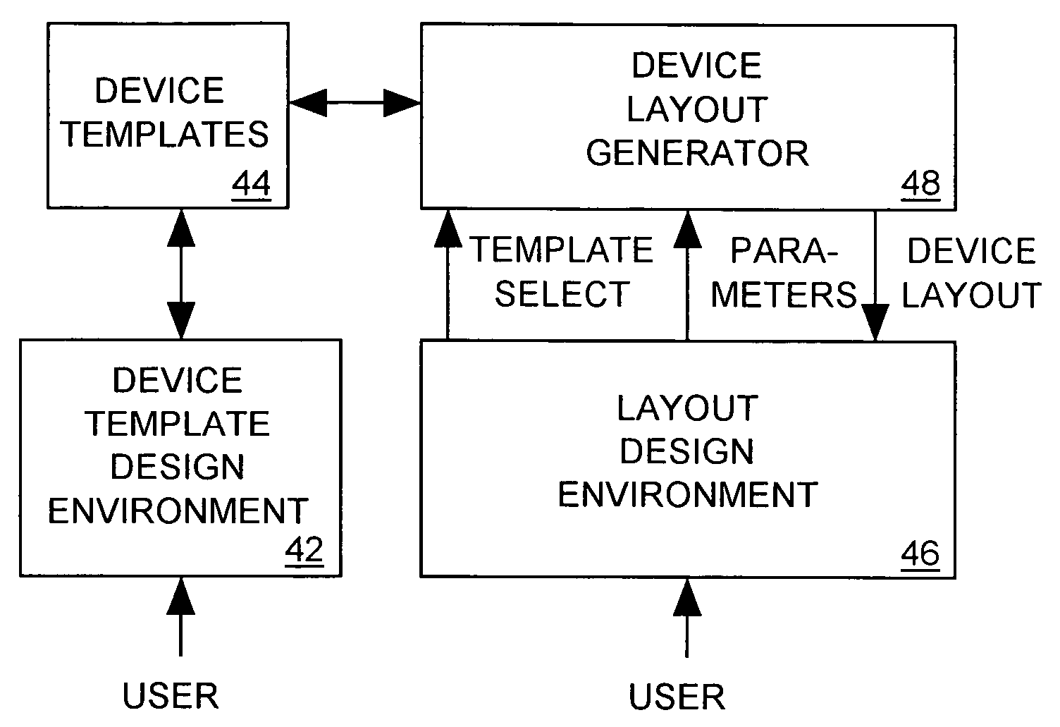
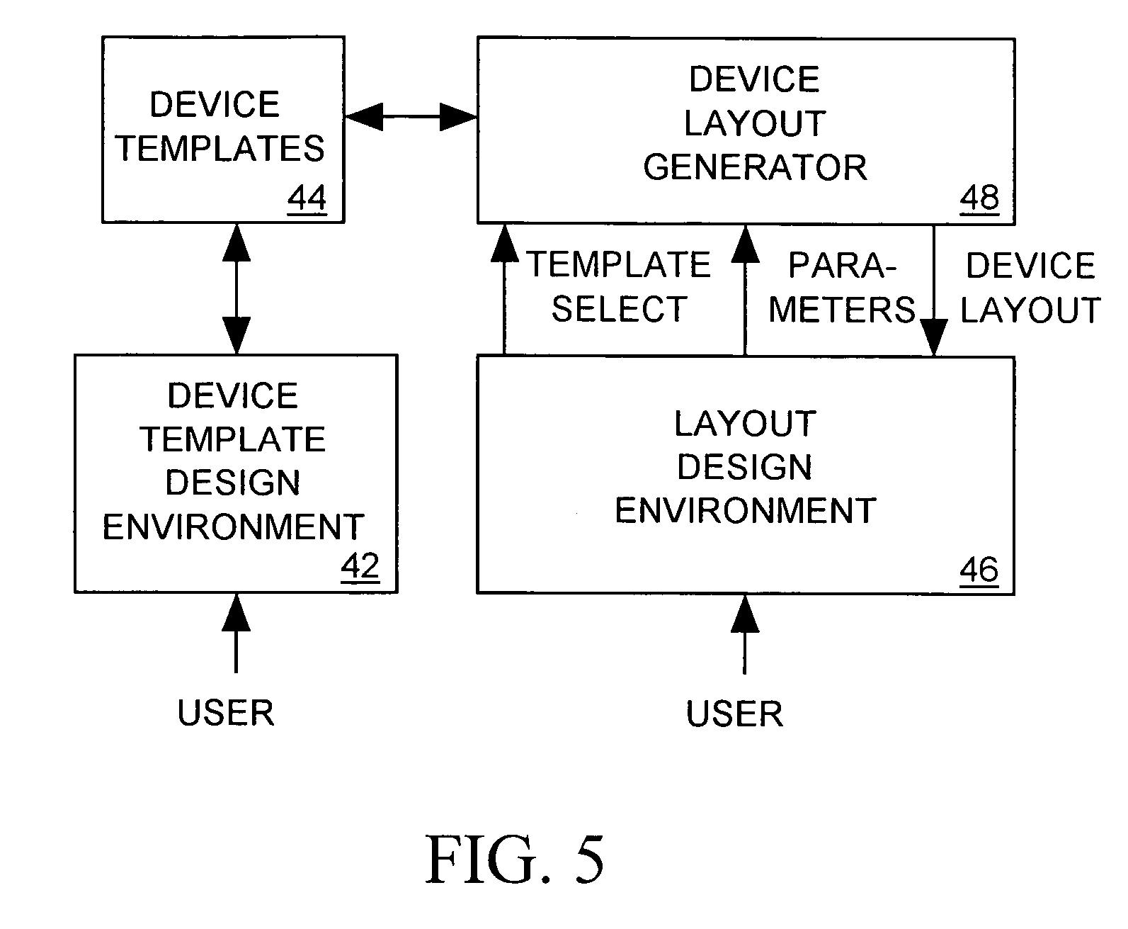
[0029]The invention relates to method for a computer-aided design (CAD) tool enabling a user to generate layouts for electronic devices incorporated into integrated circuits (ICs). The invention is suitably implemented in the form of software residing on computer-readable media which when read and executed by a conventional computer causes the computer to automatically generate electronic device layouts in response to user input. Suitable computer-readable media for storing the software include, but are not limited to, compact disks, floppy disks, hard disks, and random access or read only memory. While the specification describes at least one exemplary embodiment of the invention considered a best mode of practicing the invention, those of skill in the art will appreciate that the invention need not be limited to the particular example(s) described below or to the manner in which they operate.

[0030]An electronic device such as a transistor or a logic gate implemented within an IC i...


PUM


Abstract

A computer-aided design tool for automatically generating a layout for an electronic device to be formed by a set of objects implemented within an integrated circuit, receives input from a user defining a device template specifying shapes, dimensions and relative positions within the layout of the objects forming the device. Some of the object dimensions and / or relative positions are specified as functions of values of input parameters to be supplied by the user. When the user supplies the input parameters, the CAD tool evaluates the functions to determine the object dimensions and / or positions that are functions of the input parameters and then generates a layout for the electronic device wherein object shapes, dimensions and relative positions are as specified in the device template and consistent with the function evaluations. The device template may also include instructions for modifying the layout, for example, indicating that copies of an object are to form an array in the layout, that copies of one object are to fill another object, that an object is to be added to the layout having a shape that is a Boolean function of other objects, and that objects are to be added to or removed from the layout.

Description

CROSS-REFERENCE TO RELATED APPLICATIONS[0001]This application is a continuation-in-part of U.S. patent application Ser. No. 10 / 160,690 filed May 31, 2002 now U.S. Pat. No. 6,920,620.BACKGROUND OF THE INVENTION[0002]1. Field of the Invention[0003]The invention relates in general to a computer-aided design tool for helping an integrated circuit (IC) designer generate layouts for circuit devices implemented within an IC, and in particular to a method for producing layouts based on a scripted, hierarchical template specifying dimensions and relative positions of objects in a layout as functions of input parameters.[0004]2. Description of Related Art[0005]An IC designer typically uses computer-aided design tools to generate layouts for transistors, gates and many other types of electronic devices incorporated into an integrated circuit. For example FIG. 1 is a simplified sectional elevation view of an nMOS transistor 10 including a semiconductor substrate 11 having a p-doped well area 12...

Claims


Application Information

Patent Timeline
Patent Type & Authority Patents(United States)
IPC IPC(8): G06F17/50
CPCG06F17/5068G06F30/39
Inventor LIN, CHIA-CHIWANG, JU-CHIANCHANG, MIN-WEN
Owner SYNOPSYS INC
Why Eureka
Try Eureka