Method of manufacturing semiconductor wafer

a manufacturing method and technology of semiconductor wafers, applied in the direction of semiconductor devices, electrical equipment, basic electric elements, etc., can solve the problem that adhesion contaminants cannot be completely removed, and achieve the effect of high rigidity and high quality

Active Publication Date: 2007-02-27
DISCO CORP
View PDF3 Cites 12 Cited by
  • Summary
  • Abstract
  • Description
  • Claims
  • Application Information

AI Technical Summary

Benefits of technology

[0014]In view of the above problem, an object of the present invention is to prevent from warping in grinding a back surface of a semiconductor wafer to thin the semiconductor wafer and in forming a film in a method of manufacturing the semiconductor wafer wherein the back surface of a starting semiconductor wafer formed with circuits in a front surface thereof is ground to thin the semiconductor wafer and wherein the thin film is formed on the ground back surface. Further, another object of the invention is to prevent contaminants appeared due to a grinding work step from entering the formed film as impurities during the film formation and from degrading the quality of the film.
[0015]The method of manufacturing a semiconductor wafer according to the invention wherein a film is formed on a back surface of a starting semiconductor wafer formed with circuits in a front surface thereof, comprises a unification step of supporting a front surface of a semiconductor wafer on a support baseplate having a flat support surface, and then unifying the support baseplate and the semiconductor wafer with each other; a grinding work step of holding a support baseplate side of the unified structure on a chuck table of a grinding apparatus, and then grinding a back surface of the semiconductor wafer to thin the semiconductor wafer by grinding means of the grinding apparatus; and a film formation step of holding the support baseplate side unified with the thinned semiconductor wafer, on a chuck table of a film formation apparatus, and then forming the film on the back surface of the semiconductor wafer by film formation means of the film formation apparatus, wherein a protective tape capable of being tom off is stuck onto a back surface of the support baseplate at the unification step, so as to perform the subsequent grinding work step with the protective tape borne on the support baseplate; and a protective-tape tearing-off and removal step of tearing off and removing the protective tape is interposed before the film formation step is performed. In this way, the semiconductor wafer can be uniformly thinned without warping, and the uniform film in which no contaminants coexist can be efficiently formed on the back surface of the semiconductor wafer.
[0018]Assuming that some of the contaminants be brought into the film formation apparatus, they are scattered within the film formation apparatus upon the actuation of the film formation means under a reduced pressure, and they are deposited on the back surface of the semiconductor wafer together with a film forming substance, so that a film containing the impurities of the contaminants is partly formed. Therefore, after the cleaning step for the semiconductor wafer and the support baseplate in the unified state, and before the transportation of the unitary structure into the film formation apparatus, the protective tape polluted with the contaminants is tom off and removed. Thus, the contaminants can be completely removed from the back surface side of the support baseplate, and they are not brought into the film formation apparatus, so that the drawback ascribable to the contaminants can be eliminated at the film formation step.
[0019]As mentioned above, according to the method of manufacturing a semiconductor wafer of the invention, the grinding work step and the film formation step is implemented in a state where the starting semiconductor wafer is supported by the support baseplate of high rigidity. Therefore, even when the semiconductor wafer is worked to be as very thin as 100 μm or below at the grinding work step, a uniform film can be formed on the back surface of the semiconductor wafer without the warp of the semiconductor wafer, so that the semiconductor wafer can be thinned still further.

Problems solved by technology

The adherent contaminants cannot be completely removed even when a cleaning step is carried out after the grinding work step.

Method used


Image

  • Method of manufacturing semiconductor wafer
  • Method of manufacturing semiconductor wafer
  • Method of manufacturing semiconductor wafer

Examples


Embodiment Construction

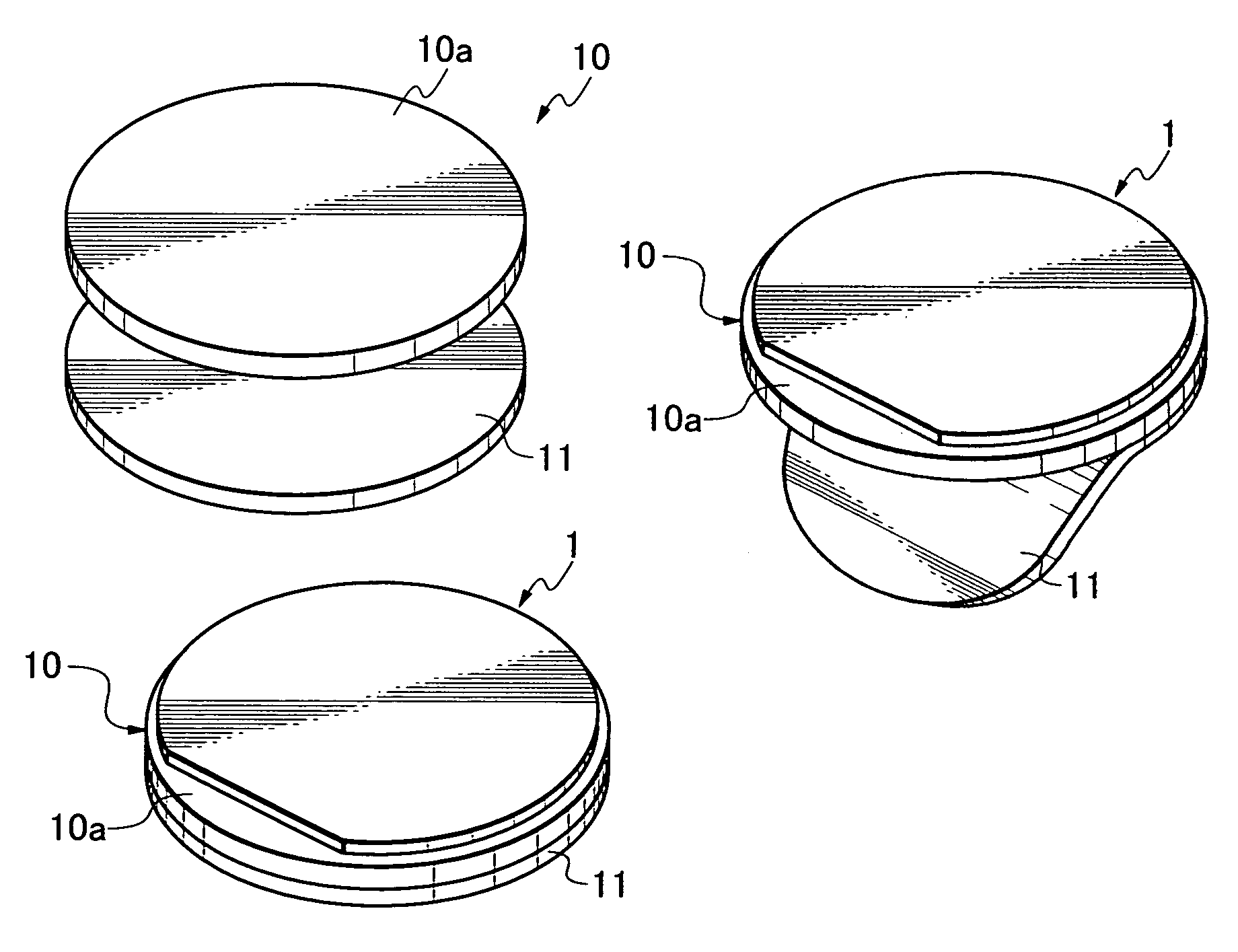
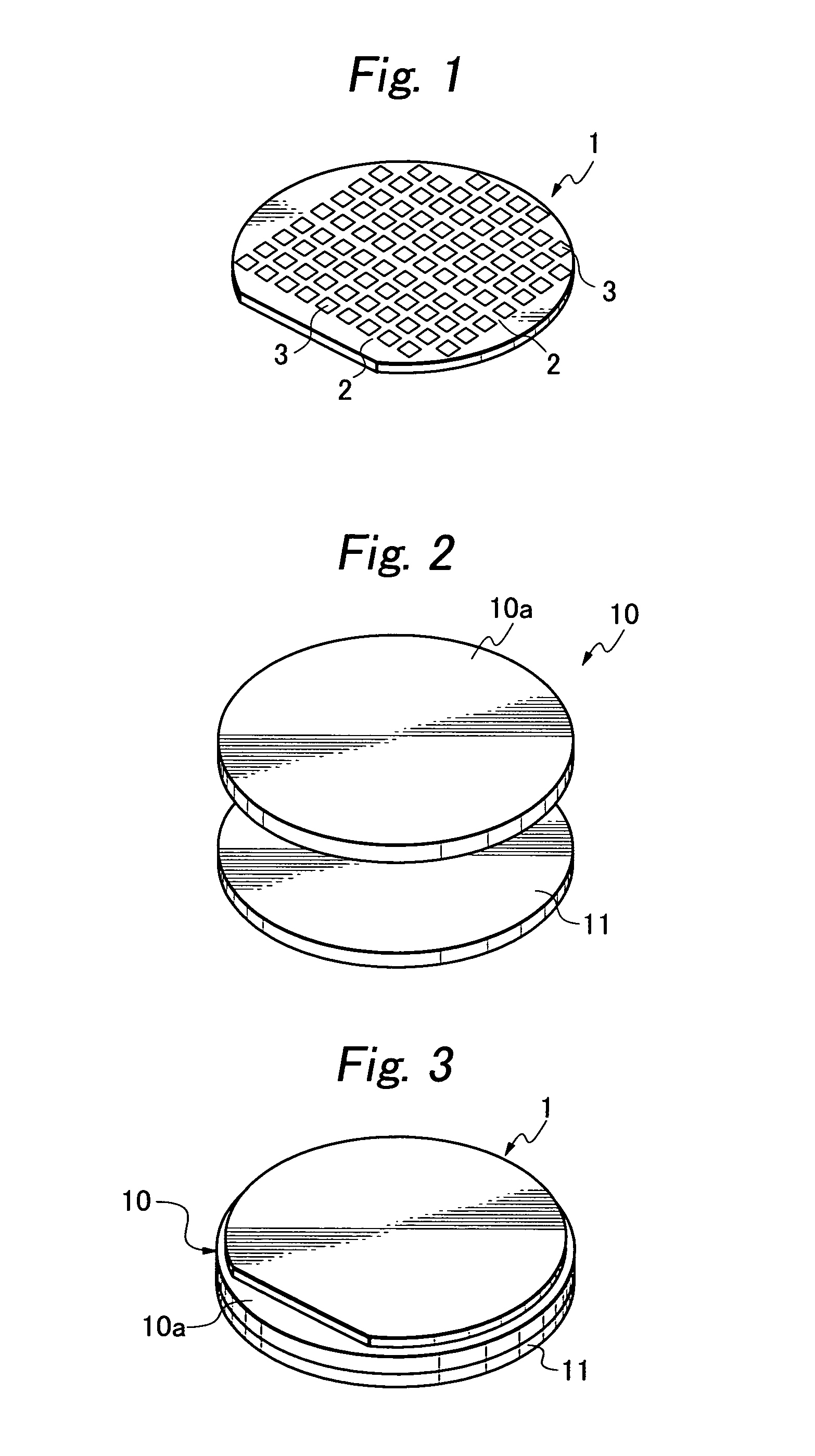
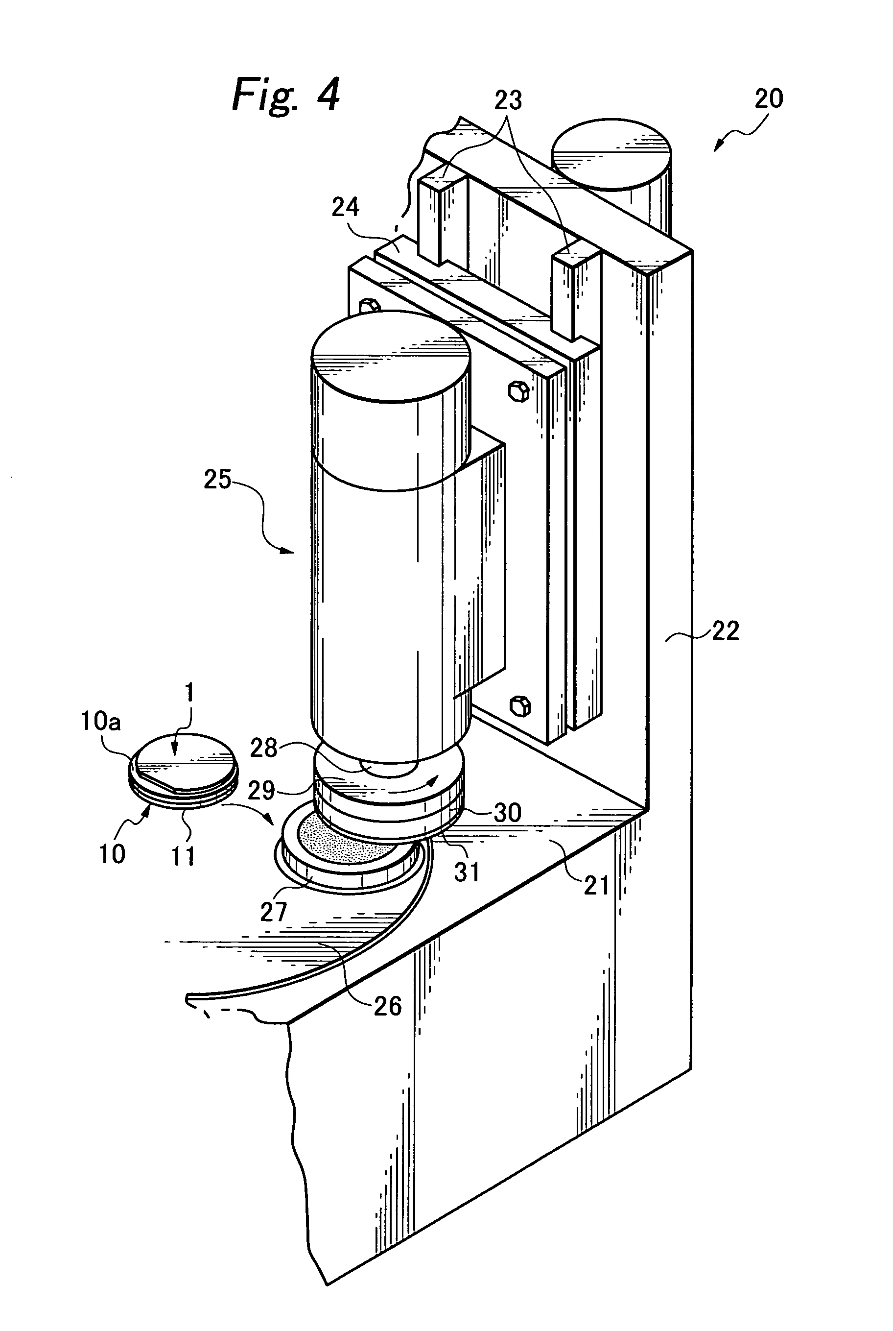
[0027]Now, a method of manufacturing a semiconductor wafer according to the present invention will be described with reference to the drawings. FIG. 1 shows a semiconductor wafer 1. There will be described a case where the back surface of the semiconductor wafer 1 is formed with a film after grinding or etching. In the front surface of the semiconductor wafer 1, a plurality of streets 2 are formed in a lattice shape at predetermined intervals, and circuit patterns are formed in a large number of rectangular regions demarcated by the streets 2. Besides, the respective rectangular regions are made into semiconductor chips 3 by dicing the streets 2.

[0028]Before the back surface of the semiconductor wafer 1 is ground or polished and is formed with the film thereon, this semiconductor wafer 1 is unified with a support baseplate 10 shown in FIG. 2. The support baseplate 10 is made of a member of high rigidity so that the semiconductor wafer 1 whose thickness has been made as very small as...


PUM

PropertyMeasurementUnit
thicknessaaaaaaaaaa
thicknessaaaaaaaaaa
thicknessaaaaaaaaaa

Abstract

A method of manufacturing a semiconductor wafer wherein a film is formed on a back surface of a starting semiconductor wafer formed with circuits in a front surface thereof. To prevent the semiconductor wafer from warping even when it is worked as very thin as 100 μm or below and to form the film uniformly on the back surface of the semiconductor wafer, the method includes a unification step of supporting the front surface of the semiconductor wafer on a support baseplate having a flat support surface, and then unifying the support baseplate and the semiconductor wafer with each other, a grinding work step of grinding the back surface of the semiconductor wafer to thin; and a film formation step of forming a film on the back surface of the semiconductor wafer with use of a film formation apparatus; wherein a protective tape capable of being tom off is stuck onto a back surface of the support baseplate at said unification step, so as to perform the subsequent grinding work step with the protective tape borne on the support baseplate; and a protective-tape tearing off and removal step of tearing off and removing the protective tape is carried out before performing said film formation step.

Description

BACKGROUND OF THE INVENTION[0001]1. Field of the Invention[0002]The present invention relates to a method of manufacturing a semiconductor wafer wherein the back surface of a starting semiconductor wafer which is formed with a plurality of semiconductor chips, for example, ICs or LSIs, in its front surface is equally ground and thinned all over by a grinding apparatus, and an oxide film or the like is thereafter formed on the ground back surface.[0003]2. Related Art[0004]A semiconductor wafer of the type specified above, formed with a plurality of semiconductor chips such as ICs or LSIs, has its back surface ground and thinned by a grinding apparatus, and the ground semiconductor wafer is thereafter split into the individual semiconductor chips by a splitting apparatus such as dicing apparatus. The semiconductor chips are assembled and extensively utilized in the circuits of electric equipments such as portable telephones and personal computers.[0005]Meanwhile, as the structures of ...

Claims


Application Information

Patent Timeline
Patent Type & Authority Patents(United States)
IPC IPC(8): H01L21/30H01L21/46H01L21/28C08J5/12H01L21/00H01L21/301H01L21/304H01L21/31H01L21/58H01L21/68H01L21/683
CPCH01L21/304H01L21/6835H01L2221/6834
Inventor ARAI, KAZUHISA
Owner DISCO CORP
Why Eureka
Try Eureka