Method of forming notched gate structure

a notched gate and structure technology, applied in the direction of basic electric elements, electrical apparatus, semiconductor devices, etc., can solve the problems of limited yield of semiconductor devices and product throughout, notched structure and size are not easily controlled, and limit the performance and electrical quality of mosfet, etc., to achieve the effect of increasing the sensitivity of doping ions

Inactive Publication Date: 2007-03-06
GRACE SEMICON MFG CORP
View PDF2 Cites 0 Cited by
  • Summary
  • Abstract
  • Description
  • Claims
  • Application Information

AI Technical Summary

Benefits of technology

[0008]The present invention provides a method of forming a notched gate structure, in which the implantation step of forming the lightly doped drain LDD benefits by increasing the sensitivity of doping ions and forming of the silicon substrate.
[0009]The present invention also provides a method of a forming notched gate structure, in which the microloading effect is reduced and the wafer to wafer stability is improved.
[0010]The present invention also provides a method of forming a notched gate structure, which reduces the resistivity of the self-aligned salicide and simplifies the controllability of the process, thereby increasing the process stability.

Problems solved by technology

As the dimension of the device shrinks to several nm, the parasitic capacitance between the gate and the source / drain extension increases in importance but limits the performance and the electrical quality of the MOSFET.
However, the notched gate structure of the conventional process uses isotropic etching.
When performing the isotropic etching, the notched structure and the size are not easily controlled due to some processes having the same etching ratio.
Therefore, the yield of the semiconductor devices and the throughout of product are limited.
The etching result is difficult of control by using the notched gate structure to reduce the parasitic capacitance between the gate and the source / drain extension.
The stability of devices are further influenced, thereby resulting in greater difficulty in fabricating the smaller semiconductor devices and reduces the yield and the electrical quality of devices.

Method used


Image

  • Method of forming notched gate structure
  • Method of forming notched gate structure
  • Method of forming notched gate structure

Examples


Embodiment Construction

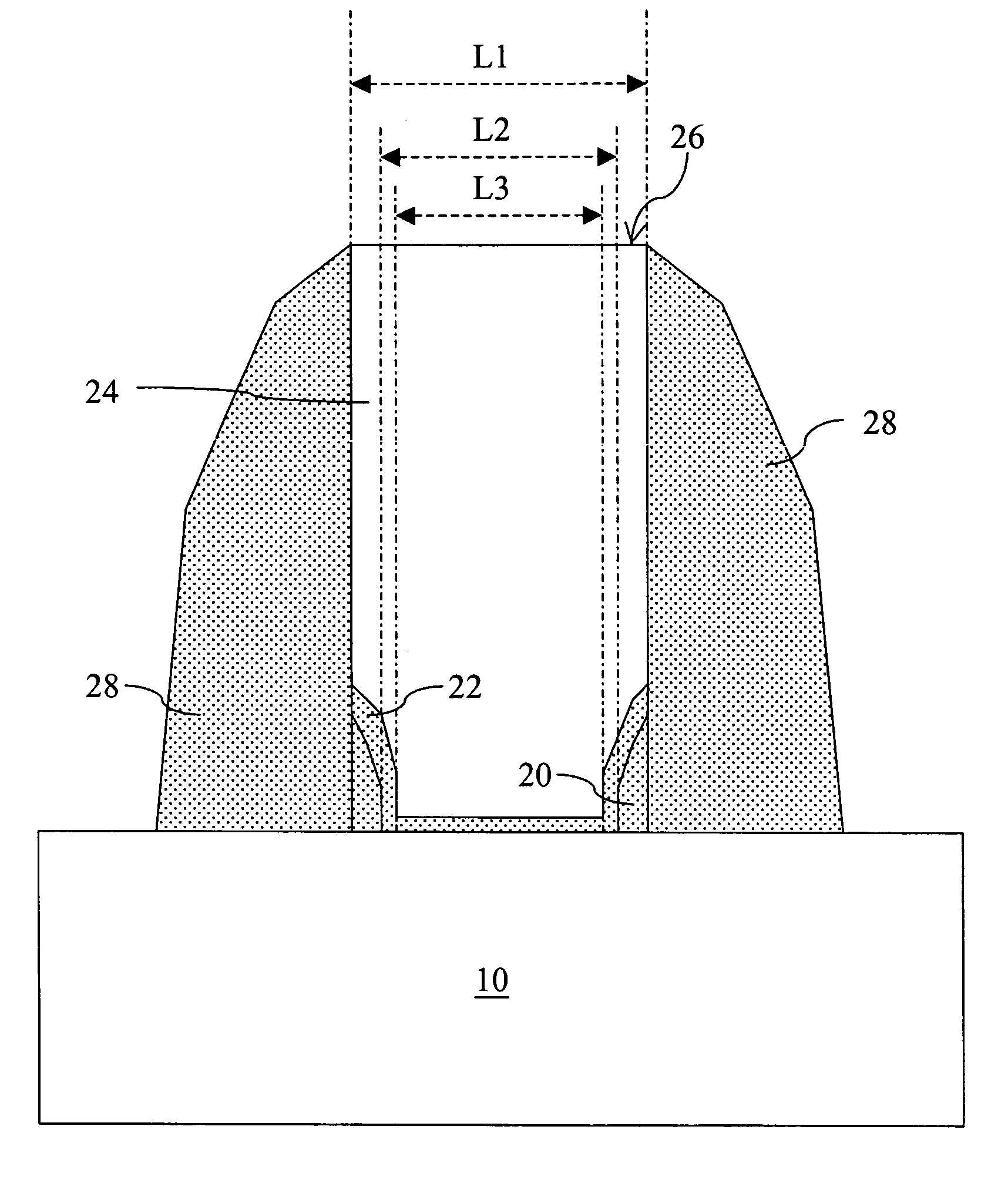
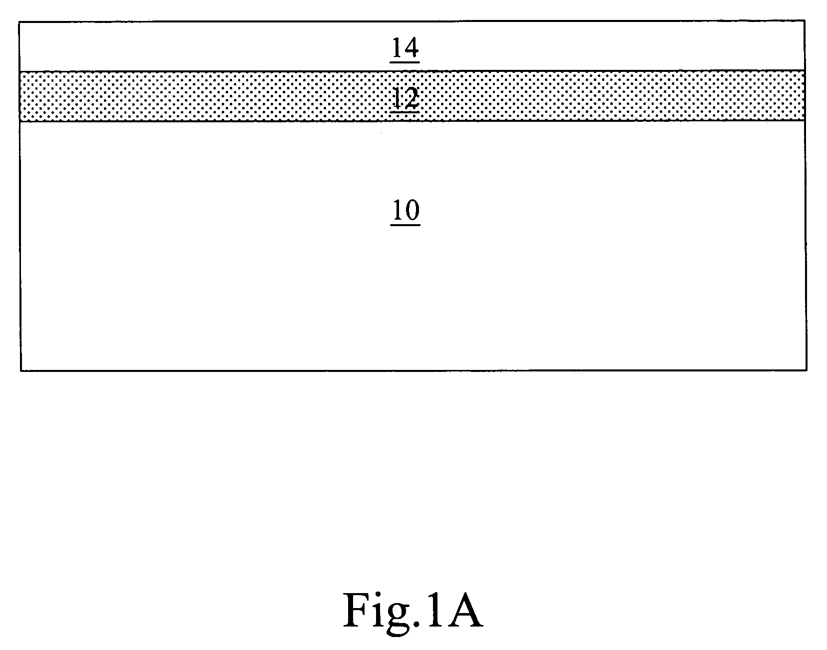
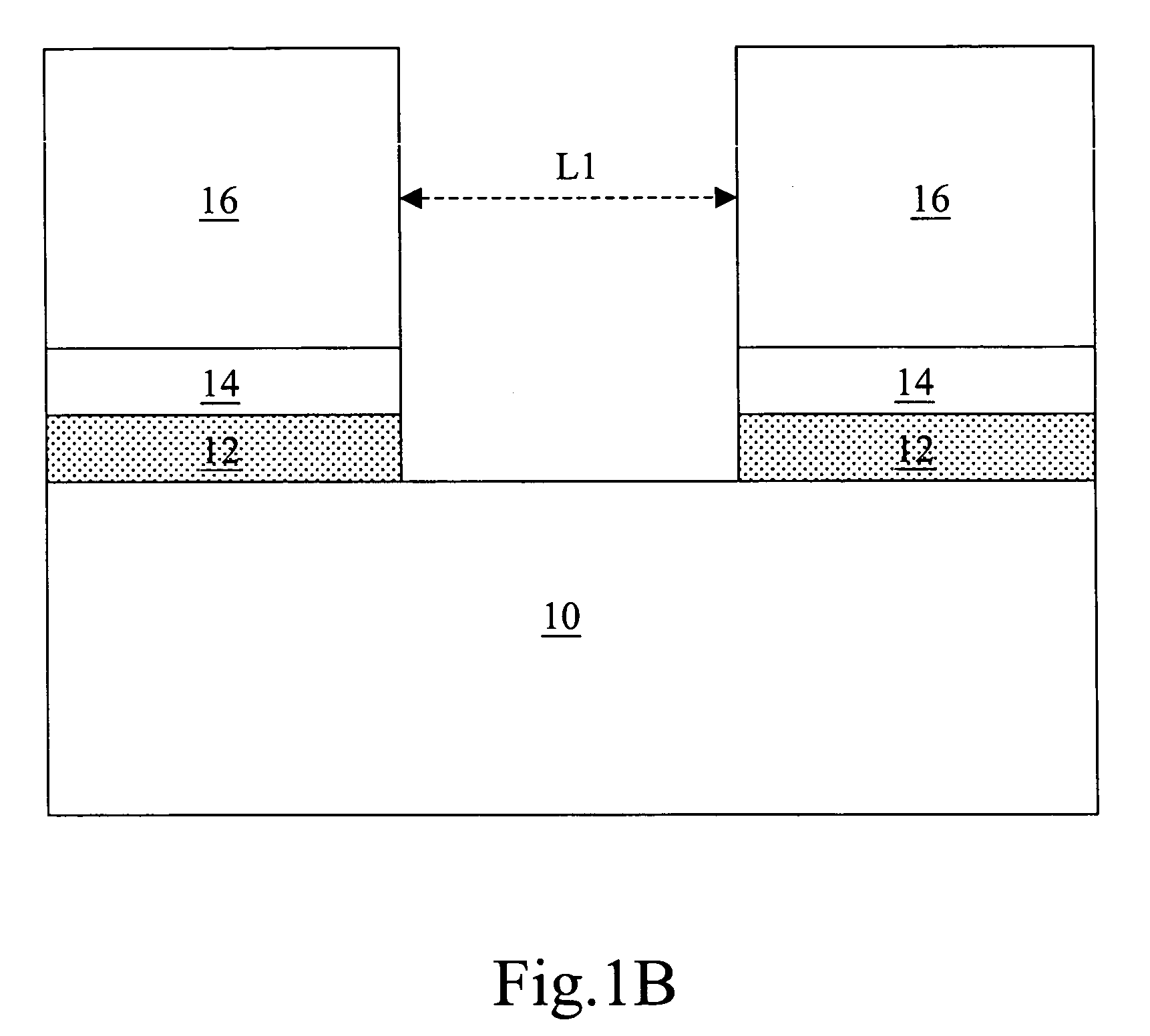
[0016]FIGS. 1A through 1G are sectional diagrams illustrating the structure of each step for forming a notched gate structure according to a preferred embodiment of the present invention. As shown in the Figures, the method of the present invention comprises; firstly, providing a semiconductor substrate 10, which is typically a silicon substrate. Refer to FIG. 1A, a first dielectric layer 12 and a first conductive layer 14 in sequence are formed on the semiconductor substrate 10 by using, for example, Chemical Vapor Deposition. The first conductive layer 14 is typically a polysilicon layer and the thickness is between 100 and 200 angstroms (Å). The doping is optional. The first dielectric layer 12 is typically an oxide layer formed on the surface of the silicon substrate and the thickness is about 100 angstroms. The properly isolation structure or the doped area is formed in the semiconductor substrate 10 (not shown in the drawing), for example, a field oxide layer, a shallow trench...


PUM


Abstract

A method of forming a notched gate structure comprising a semiconductor substrate having a first oxide layer formed thereon. A first conductive layer is formed on the semiconductor substrate. A portion of the first conductive layer and a portion of the first oxide layer are removed to form first gate structures. First spacers are formed on the sidewalls of the gate structure. A second oxide layer is formed on the semiconductor substrate. A second conductive layer is formed on the surface of the second oxide layer. The first gate structures and the second conductive layer formed thereon are then removed to form a second gate structure. Second spacers are formed on the sidewalls of the second gate structure to complete the notched gate structure process. The method of the present invention reduces the capacitance between the gate and the source / drain extension, and simplifies the process, thereby increasing the controllability of the process.

Description

BACKGROUND OF THE INVENTION[0001]1. Field of the Invention[0002]The present invention relates to a method of forming a gate structure, and more particularly, to a method of forming a notched gate structure.[0003]2. Description of the Prior Art[0004]The accelerating rate of improvement in the performance of advanced generations of CMOS IC's has been enabled by the aggressive scaling of the minimum lithographic feature size and supply voltages as well as innovations in transistor structure, and the addition of higher-levels of systems functionality of the IC design.[0005]Fabrication of a metal oxide semiconductor field-effect transistor (“MOSFET”) device is well known. As the dimension of the device shrinks to several nm, the parasitic capacitance between the gate and the source / drain extension increases in importance but limits the performance and the electrical quality of the MOSFET. Therefore, a notched gate structure is provided in order to reduce the parasitic capacitance between...

Claims


Application Information

Patent Timeline
Patent Type & Authority Patents(United States)
IPC IPC(8): H01L21/338
CPCH01L21/28114H01L29/42376H01L29/66583H01L29/66553H01L29/513
Inventor HUH, YUN JUN
Owner GRACE SEMICON MFG CORP
Why Eureka
Try Eureka